TLE9263QX
System Features
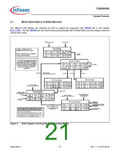
5.1.1
Device Configuration and SBC Init Mode
The SBC starts up in SBC Init Mode after crossing the power-on reset VPOR,r threshold (see also Chapter 15.3)
and the watchdog will start with a long open window (tLW).
During this power-on phase following configurations are stored in the device:
•
•
The device behavior regarding a watchdog trigger failure and a VCC1 over voltage condition is determined by
the external circuitry on the INT pin (see below)
The selection of the normal device operation or the SBC Software Development Mode (watchdog disabled for
debugging purposes) will be set depending on the voltage level of the FO3/TEST pin (see also Chapter 5.1.7).
5.1.1.1
Device Configuration
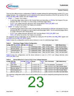
The configuration selection is intended to select the SBC behavior regarding a watchdog trigger failure. Depending
on the requirements of the application, the VCC1 output shall be switched OFF and the device shall go to SBC
Fail-Safe Mode in case of a watchdog failure (1 or 2 fails). To set this configuration (Config 2/4), the INT pin does
not need an external pull-up resistor. In case VCC1 should not be switched OFF (Config 1/3), the INT pin needs
to have an external pull-up resistor connected to VCC1 (see application diagram in Chapter 17.1).
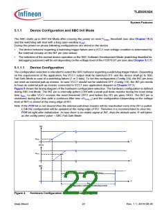
Figure 5 shows the timing diagram of the hardware configuration selection. The hardware configuration is defined
during SBC Init Mode. The INT pin is internally pulled LOW with a weak pull-down resistor during the reset delay
time tRD1, i.e.after VCC1 crosses the reset threshold VRT1 and before the RO pin goes HIGH. The INT pin is
monitored during this time (with a continuos filter time of tCFG_F) and the configuration (depending on the voltage
level at INT) is stored at the rising edge of RO.
Note:If the POR bit is not cleared then the internal pull-down resistor will be reactivated every time RO is pulled
LOW the configuration will be updated at the rising edge of RO. Therefore it is recommended to clear the
POR bit right after initialization. In case there is no stable signal at INT, then the default value ‘0’ will taken
as the config select value = SBC Fail-Safe Mode.
VS
VPOR,r
t
VCC1
VRT1,r
t
RO
tCFG_F
Continuous Filtering with
t
tRD1
Configuration selection monitoring period
Figure 4
Hardware Configuration Selection Timing Diagram
Data Sheet
22
Rev. 1.1, 2014-09-26

 INFINEON [ Infineon ]