TC1796
Functional Description
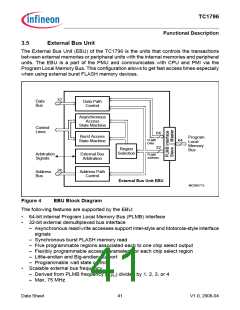
3.4
Memory Protection System
The TC1796 memory protection system specifies the addressable range and read/write
permissions of memory segments available to the currently executing task. The memory
protection system controls the position and range of addressable segments in memory.
It also controls the kinds of read and write operations allowed within addressable
memory segments. Any illegal memory access is detected by the memory protection
hardware, which then invokes the appropriate Trap Service Routine (TSR) to handle the
error. Thus, the memory protection system protects critical system functions against both
software and hardware errors. The memory protection hardware can also generate
signals to the Debug Unit to facilitate tracing illegal memory accesses.
There are two Memory Protection Register Sets in the TC1796, numbered 0 and 1,
which specify memory protection ranges and permissions for code and data. The
PSW.PRS bit field determines which of these is the set currently in use by the CPU.
Because the TC1796 uses a Harvard-style memory architecture, each Memory
Protection Register Set is broken down into a Data Protection Register Set and a Code
Protection Register Set. Each Data Protection Register Set can specify up to four
address ranges to receive particular protection modes. Each Code Protection Register
Set can specify up to two address ranges to receive particular protection modes.
Each of the Data Protection Register Sets and Code Protection Register Sets
determines the range and protection modes for a separate memory area. Each contains
register pairs which determine the address range (the Data Segment Protection
Registers and Code Segment Protection Registers) and one register (Data Protection
Mode Register) which determines the memory access modes which apply to the
specified range.
Data Sheet
40
V1.0, 2008-04

 INFINEON [ Infineon ]