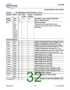
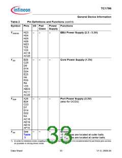
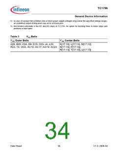
TC1796
Functional Description
3
Functional Description
The following section gives an overview of the sub systems and the modules of the
TC1796 and their connectivity.
3.1
System Architecture and On-Chip Bus Systems
The TC1796 has four independent on-chip buses (see also TC1796 block diagram in
Figure 1):
•
•
•
•
Program Local Memory Bus (PLMB)
Data Local Memory Bus (DLMB)
System Peripheral Bus (SPB)
Remote Peripheral Bus (RPB)
The two LMB Buses (Program Local Memory Bus PLMB and Data Local Memory Bus
DLMB) connect the TriCore CPU to its local resources for data and instruction fetches.
The PLMB/DLMB Buses are synchronous and pipelined buses with variable block size
transfer support. The protocol supports 8-, 16-, 32-, and 64-bit single transactions and
variable length 64-bit block transfers.
The System Peripheral Bus (SPB) is accessible by the CPU via the LFI Bridge. The
LFI Bridge is a bi-directional bus bridge between the DLMB and the SPB. It supports all
transactions types of both buses, DLMB Bus and FPI Bus. It handles address translation
and transaction type translation between the two buses. The LFI Bridge further supports
the pipelining of both connected buses. Therefore, no additional delay is created except
for bus protocol conversions.
The Remote Peripheral Bus (RPB) connects the peripherals with high data rates (SSC,
ADC, FADC) with the Dual-port memory (DPRAM) in the DMI, relieving the SPB and the
PLMB/DLMB Buses from these data transfers. The RPB is controlled by a bus switch
which is located in the DMA controller.
The two LMB Buses are running at CPU clock speed (clock rate of fCPU) while SPB and
RPB are running at system clock speed (clock rate of fSYS). Note that fSYS can be equal
to fCPU or half the fCPU frequency.
Data Sheet
36
V1.0, 2008-04

 INFINEON [ Infineon ]