TC1796
Electrical Parameters
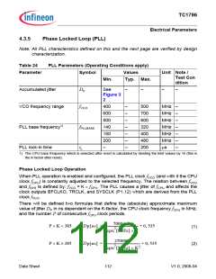
4.3.6
BFCLKO Output Clock Timing
VSS = 0 V;VDD = 1.5 V ± 5%; VDDEBU = 2.5 V ± 5% and 3.3 V ± 5%;
TA = -40 °C to +125 °C; CL = 35 pF
Table 25
BFCLK0 Output Clock Timing Parameters1)
Parameter
Symbol
Values
Typ. Max.
Unit Note /
Test Con
Min.
dition
BFCLKO clock period
BFCLKO high time
BFCLKO low time
BFCLKO rise time
BFCLKO fall time
t
BFCLKO CC 13.332)
–
–
–
–
–
50
–
–
–
3
3
55
ns
ns
ns
ns
ns
%
–
–
–
–
–
t5
t6
t7
t8
CC 3
CC 3
CC –
CC –
BFCLKO duty cycle t5/(t5 + t6)3) DC24 CC 45
divider of
2, 4, ...4)
BFCLKO duty cycle t5/(t5 + t6)3) DC3 CC 30
33.33 36
%
divider of
3 4)
BFCLKO high time reduction5) dt5
1) Not subject to production test, verified by design/characterization.
CC –
–
1.1
ns
CL = 20pF
2) The PLL jitter characteristics add to this value according to the application settings. See the PLL jitter
parameters.
3) The PLL jitter is not included in this parameter. If the BFCLKO frequency is equal to fCPU, the K-divider setting
determines the duty cycle.
4) The division ratio between LMB and BFCLKO frequency is set by EBU_BFCON.EXTCLOCK.
5) Due to asymmetry of the delays and slopes of the rising and falling edge of the pad. The influence of the PLL
jitter is included in this parameter. This parameter should be applied taking the typical value of the duty cycle
in the account, not the minimum or maximum value.
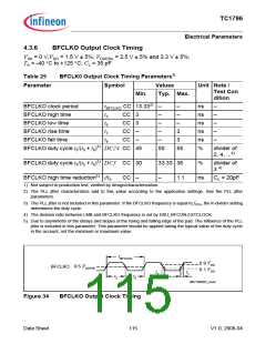
tBFCLKO
0.9 VDD
0.5 VDDP05
BFCLKO
0.1 VDD
t8
t7
t5
t6
MCT04883_mod
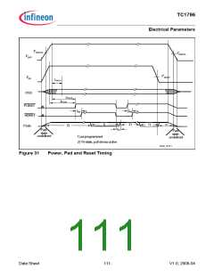
Figure 34
BFCLKO Output Clock Timing
Data Sheet
115
V1.0, 2008-04

 INFINEON [ Infineon ]