TC1796
Electrical Parameters
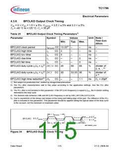
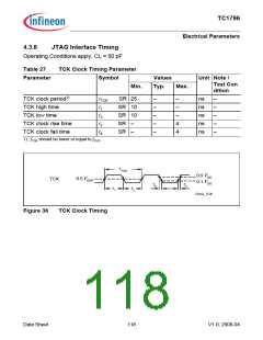
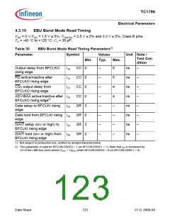
Table 28
Parameter
JTAG Timing Parameters1)
Symbol
Values
Typ. Max.
Unit Note /
Test Con
dition
Min.
TMS setup to TCK rising edge t1
SR 6.0
–
–
–
–
–
–
–
–
–
–
–
13
–
14
ns
ns
ns
ns
ns
ns
ns
–
–
–
–
TMS hold to TCK rising edge
TDI setup to TCK rising edge
TDI hold to TCK rising edge
t2
t1
t2
t3
t3
t4
SR 6.0
SR 6.0
SR 6.0
CC –
CC 3.0
CC –
TDO valid output from TCK
CL = 50 pF
CL = 20 pF
CL = 50 pF
falling edge2)
TDO high impedance to valid
output from TCK falling edge2)
TDO valid output to high
impedance from TCK falling
edge2)
t5
CC –
–
13.5
ns
CL = 50 pF
1) fTCK should be lower or equal to fSYS
.
2) The falling edge on TCK is used to capture the TDO timing.
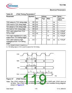
TCK
t1
t1
t2
t2
TMS
TDI
t4
t3
t5
TDO
Jtag
Figure 37
JTAG Timing
Note: The JTAG module is fully compliant with IEEE1149.1-2000 with JTAG clock at
20 MHz. The JTAG clock at 40MHz is possible with the modified timing diagram
shown in Figure 37.
Data Sheet
119
V1.0, 2008-04

 INFINEON [ Infineon ]