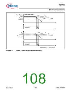
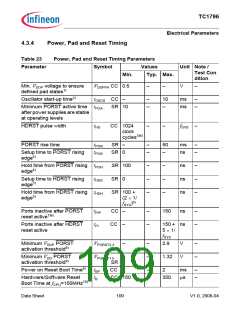
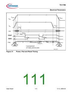
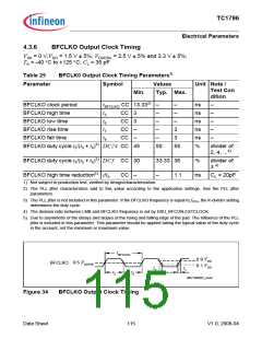
TC1796
Electrical Parameters
4.3.5
Phase Locked Loop (PLL)
Note: All PLL characteristics defined on this and the next page are verified by design
characterization.
Table 24
PLL Parameters (Operating Conditions apply)
Parameter
Symbol
Values
Typ. Max.
Unit Note /
Test Con
Min.
dition
Accumulated jitter
DP
See
–
–
–
–
Figure 3
2
VCO frequency range
fVCO
400
600
500
140
150
200
–
–
–
–
–
–
–
–
500
700
600
320
400
480
200
MHz –
MHz –
MHz –
MHz –
MHz –
MHz –
PLL base frequency1)
fPLLBASE
PLL lock-in time
tL
µs
–
1) The CPU base frequency which is selected after reset is calculated by dividing the limit values by 16 (this is
the K factor after reset).
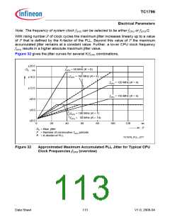
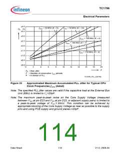
Phase Locked Loop Operation
When PLL operation is enabled and configured, the PLL clock fVCO (and with it the CPU
clock fCPU) is constantly adjusted to the selected frequency. The relation between fVCO
and fSYS is defined by: fVCO = K × fCPU. The PLL causes a jitter of fCPU and affects the
clock outputs BFCLKO, TRCLK, and SYSCLK (P1.12) which are derived from the PLL
clock fVCO
.
There will be defined two formulas that define the (absolute) approximate maximum
value of jitter DP in ns dependent on the K-factor, the CPU clock frequency fCPU in MHz,
and the number P of consecutive fCPU clock periods.
7000 × P
P × K < 385
Dp[ns] = ------------------------------------------ + 0, 535
fcpu2[MHz] × K
(1)
(2)
2700000
P × K ≥ 385
Dp[ns] = --------------------------------------------- + 0 , 5 3 5
fcpu2[MHz] × K2
Data Sheet
112
V1.0, 2008-04

 INFINEON [ Infineon ]