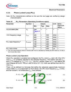
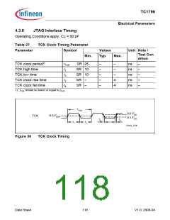
TC1796
Electrical Parameters
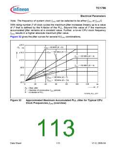
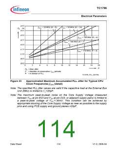
±4.0
ns
±3.5
fCPU = 50 MHz (K = 8)
fCPU = 50 MHz (K = 14)
DP
±3.0
±2.5
±2.0
±1.5
±1.0
±0.5
±0.0
fCPU = 100 MHz (K = 4)
fCPU = 100 MHz (K = 7)
fCPU = 150 MHz (K = 4)
0
2
4
6
8
10
12
14
16
18
20
P
DP
= Max. jitter
P
= Number of consecutive fCPU periods
K
= K-divider of PLL
TC1976_PLL_DETAIL
Figure 33
Approximated Maximum Accumulated PLL Jitter for Typical CPU
Clock Frequencies fCPU (detail)
Note: The specified PLL jitter values are valid if the capacitive load at the External Bus
Unit (EBU) is limited to CL=20pF.
Note: The maximum peak-to-peak noise on the Core Supply Voltage (measured
between VDD at pin E23 and VSS at pin D23, or adjacent supply pairs) is limited to
a peak-to-peak voltage of VPP = 30mV. This condition can be achieved by
appropriate blocking of the Core Supply Voltage as near as possible to the supply
pins and using PCB supply and ground planes.=20pF.
Data Sheet
114
V1.0, 2008-04

 INFINEON [ Infineon ]