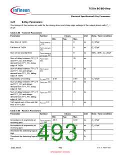
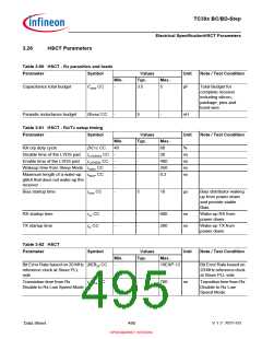
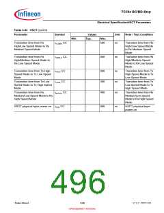
TC39x BC/BD-Step
Electrical SpecificationE-Ray Parameters
3.25
E-Ray Parameters
The timings of this section are valid for the strong driver and sharp edge settings of the output drivers with CL =
25 pF.
Table 3-58 Transmit Parameters
Parameter
Symbol
Values
Typ.
Unit
Note / Test Condition
Min.
Max.
Rise time of TxEN
Fall time of TxEN
tdCCTxENRise2
5 CC
-
-
-
-
-
9
ns
ns
ns
ns
CL=25pF
tdCCTxENFall25
CC
-
-
-
9
CL=25pF
Sum of rise and fall time
tdCCTxRise25+d
CCTxFall25 CC
9
20% - 80% ; CL=25pF
Sum of delay between TP1_FF tdCCTxEN01
25
and TP1_CC and delays
derived from TP1_FFi, rising
edge of TxEN
CC
Sum of delay between TP1_FF tdCCTxEN10
-
-
25
ns
and TP1_CC and delays
derived from TP1_FFi, falling
edge of TxEN
CC
Asymmetry of sending
t
tx_asym CC -2.45
-
-
2.45
25
ns
ns
CL=25pF
Sum of delay between TP1_FF tdCCTxD01 CC -
and TP1_CC and delays
derived from TP1_FFi, rising
edge of TxD
Sum of delay between TP1_FF tdCCTxD10 CC -
and TP1_CC and delays
derived from TP1_FFi, falling
edge of TxD
-
-
25
9
ns
ns
TxD signal sum of rise and fall
time at TP1_BD
t
txd_sum CC
-
Table 3-59 Receive Parameters
Parameter
Symbol
Values
Unit
Note / Test Condition
Min.
Typ.
Max.
Acceptance of asymmetry at
receiving part
tdCCTxAsymAcc -30.5
ept25 SR
-
43.0
ns
ns
%
%
CL=25pF
CL=15pF
Acceptance of asymmetry at
receiving part
tdCCTxAsymAcc -31.5
ept15 SR
-
-
-
44.0
70
Threshold for detecting logical TuCCLogic1
high SR
Threshold for detecting logical TuCCLogic0
35
30
65
low
SR
Data Sheet
493
V 1.2, 2021-03
OPEN MARKET VERSION

 INFINEON [ Infineon ]