TC39x BC/BD-Step
Electrical SpecificationMSC Timing 5 V Operation
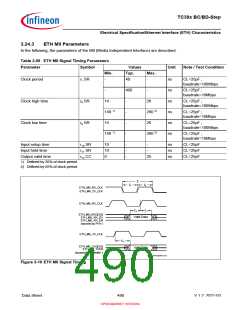
3.23
MSC Timing 5 V Operation
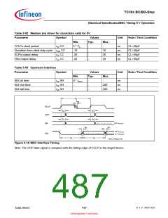
The following section defines the timings.
Note:Pad asymmetry is already included in the following timings.
Note:Load for LVDS pads are defined as differential loads in the following timings.
Table 3-49 LVDS clock/data (LVDS pads in LVDS mode) valid for 5V
Parameter
Symbol
Values
Typ.
Unit
Note / Test Condition
Min.
Max.
1) 2)
FCLPx clock period
t
40 CC
2 * TA
-
-
ns
LVDS; CL=50pF
3)
Deviation from ideal duty cycle
SOPx output delay
t
t
t
400 CC
44 CC
45 CC
-1 3)
-3 3)
-4 3)
-
-
-
1 3)
3 3)
5 3)
ns
ns
ns
LVDS; 0 < CL < 50pF
CL=50pF
ENx output delay
ss; CL=50pF; ABRA
block bypassed
-4 3)
-
4 3)
ns
ss; CL=50pF; ABRA
block used
-2 3)
-30 3)
-
-
10 3)
30 3)
ns
ns
sm; CL=50pF
m; CL=50pF
1) TA depends on the clock source selected for baud rate generation in the ABRA block of the MSC.
2) The capacitive load on the LVDS pins is differential, the capacitive load on the CMOS pins is single ended.
3) The load (CL=50pF) defined in the condition list is a load definition for the single end signal EN and does not intend to add an
additional load inside the differential signal lines. For single end signals the load definition defines the max length of the signal
on the PCB layout. For the LVDS pads the IEEE Std 1596.3-1996 load definitions apply.
Table 3-50 Strong sharp (ss) driver for clock/data valid for 5V
Parameter
Symbol
Values
Typ.
Unit
Note / Test Condition
Min.
2 * TA
-2
Max.
-
FCLPx clock period
t
t
t
t
40 CC
400 CC
44 CC
45 CC
-
-
-
-
ns
ns
ns
ns
CL=50pF
CL=50pF
CL=50pF
CL=50pF
Deviation from ideal duty cycle
SOPx output delay
2
-4
3.5
3.5
ENx output delay
-4
Table 3-51 Strong medium (sm) driver for clock/data valid for 5V
Parameter
Symbol
Values
Typ.
Unit
Note / Test Condition
Min.
2 * TA
-5
Max.
FCLPx clock period
t
t
t
t
40 CC
400 CC
44 CC
45 CC
-
-
-
-
-
ns
ns
ns
ns
CL=50pF
CL=50pF
CL=50pF
CL=50pF
Deviation from ideal duty cycle
SOPx output delay
5
7
7
-7
ENx output delay
-7
Data Sheet
486
V 1.2, 2021-03
OPEN MARKET VERSION

 INFINEON [ Infineon ]