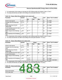
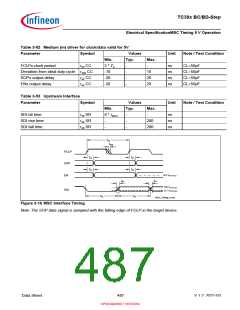
TC39x BC/BD-Step
Electrical SpecificationQSPI Timings, Master and Slave Mode
1) For compensation of the average on-chip delay the QSPI module provides the bit fields ECONz.A, B and C.
2) The setup and hold times are valid for both settings of the input pads thresholds: TTL and AL.
Table 3-46 Master Mode Strong Medium (sm) output pads
Parameter
Symbol
Values
Typ.
Unit
Note / Test Condition
Min.
50
Max.
SCLKO clock period
t
t
50 CC
-
-
-
ns
ns
CL=50pF
CL=50pF
Deviation from the ideal duty
cycle
500 CC
-5
5
MTSR delay from SCLKO
shifting edge
t
51 CC
-7
-
-
-
-
7
7
-
ns
ns
ns
ns
CL=50pF
CL=50pF
CL=50pF
CL=50pF
SLSOn deviation from the ideal t510 CC
programmed position
-7
MRST setup to SCLK latching
edge
t
52 SR
35 1) 2)
-5 1)2)
MRST hold from SCLK latching t53 SR
-
edge
1) For compensation of the average on-chip delay the QSPI module provides the bit fields ECONz.A, B and C.
2) The setup and hold times are valid for both settings of the input pads thresholds: TTL and AL.
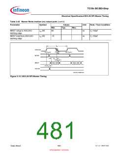
Table 3-47 Master Mode Medium (m) output pads
Parameter
Symbol
Values
Typ.
Unit
Note / Test Condition
Min.
160
-10
Max.
-
SCLKO clock period
t
t
50 CC
-
-
ns
ns
CL=50pF
CL=50pF
Deviation from the ideal duty
cycle
500 CC
10
MTSR delay from SCLKO
shifting edge
t
51 CC
-20
-
-
-
20
20
-
ns
ns
ns
CL=50pF
CL=50pF
CL=50pF
SLSOn deviation from the ideal t510 CC
programmed position
-20
MRST setup to SCLK latching
edge
t
52 SR
80 1) 2)
MRST hold from SCLK latching t53 SR
edge
-15 1)2)
-13 1)2)
-
-
-
-
ns
ns
CL=50pF
CL=50pF; SCR SSC
1) For compensation of the average on-chip delay the QSPI module provides the bit fields ECONz.A, B and C.
2) The setup and hold times are valid for both settings of the input pads thresholds: TTL and AL.
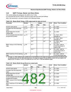
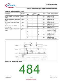
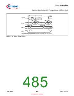
Table 3-48 Slave mode timing
Parameter
Symbol
Values
Typ.
Unit
Note / Test Condition
Min.
Max.
-
SCLK clock period
SCLK duty cycle
t
t
54 SR
4 x TMAX
40
-
-
ns
%
55/t54 SR
60
Data Sheet
483
V 1.2, 2021-03
OPEN MARKET VERSION

 INFINEON [ Infineon ]