TC39x BC/BD-Step
Electrical SpecificationASCLIN SPI Master Timing
3.21
ASCLIN SPI Master Timing
This section defines the timings for the ASCLIN in the TC39x.
Note:Pad asymmetry is already included in the following timings.
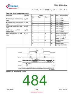
Table 3-41 Master Mode strong sharp (ss) output pads
Parameter
Symbol
Values
Typ.
Unit
Note / Test Condition
Min.
20
Max.
ASCLKO clock period
t
t
t
50 CC
500 CC
51 CC
-
-
-
-
ns
ns
ns
CL=25pF
CL=25pF
CL=25pF
Deviation from ideal duty cycle
-2
2
MTSR delay from ASCLKO
shifting edge
-3.5
3.5
ASLSOn delay from the first
ASCLKO edge
t
t
t
510 CC
52 SR
53 SR
-3
25
-2
-
-
-
3.5
ns
ns
ns
CL=25pF
CL=25pF
CL=25pF
MRST setup to ASCLKO
latching edge
-
-
MRST hold from ASCLKO
latching edge
Table 3-42 Master Mode strong medium (sm) output pads
Parameter
Symbol
Values
Typ.
Unit
Note / Test Condition
Min.
50
Max.
ASCLKO clock period
t
t
t
50 CC
500 CC
51 CC
-
-
-
-
ns
ns
ns
CL=50pF
CL=50pF
CL=50pF
Deviation from ideal duty cycle
-5
5
7
MTSR delay from ASCLKO
shifting edge
-7
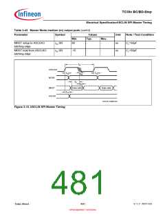
ASLSOn delay from the first
ASCLKO edge
t
t
t
510 CC
52 SR
53 SR
-7
35
-5
-
-
-
7
-
ns
ns
ns
CL=50pF
CL=50pF
CL=50pF
MRST setup to ASCLKO
latching edge
MRST hold from ASCLKO
latching edge
-
Table 3-43 Master Mode medium (m) output pads
Parameter
Symbol
Values
Unit
Note / Test Condition
Min.
160
-10
Typ.
Max.
-
ASCLKO clock period
t
t
t
50 CC
500 CC
51 CC
-
-
-
ns
ns
ns
CL=50pF
CL=50pF
CL=50pF
Deviation from ideal duty cycle
10
20
MTSR delay from ASCLKO
shifting edge
-20
ASLSOn delay from the first
ASCLKO edge
t
510 CC
-20
-
20
ns
CL=50pF
Data Sheet
480
V 1.2, 2021-03
OPEN MARKET VERSION

 INFINEON [ Infineon ]