TC39x BC/BD-Step
Pin Definition and Functions: LFBGA-516 Package Variant Pin Configuration
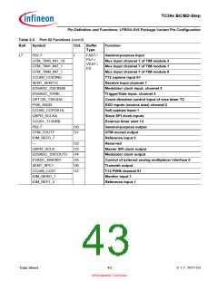
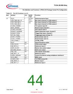
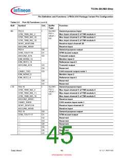
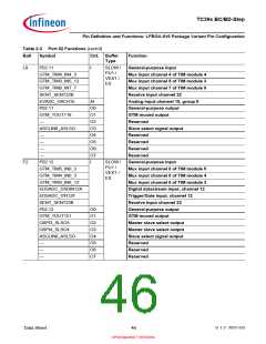
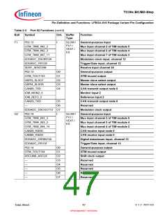
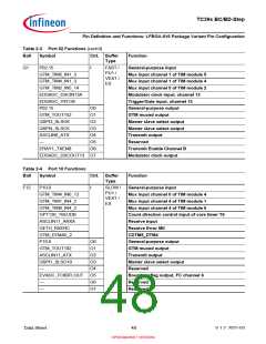
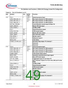
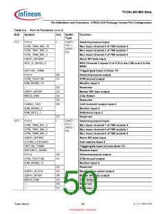
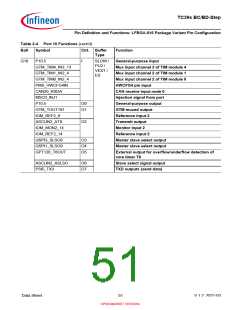
Table 2-3 Port 02 Functions (cont’d)
Ball
Symbol
Ctrl. Buffer
Type
Function
F1
P02.13
I
SLOW /
PU1 /
VEXT /
ES
General-purpose input
Mux input channel 2 of TIM module 5
Mux input channel 2 of TIM module 4
Mux input channel 7 of TIM module 3
Modulator clock input, channel 12
Trigger/Gate input, channel 12
Receive input channel 24
General-purpose output
GTM muxed output
GTM_TIM5_IN2_2
GTM_TIM4_IN2_3
GTM_TIM3_IN7_11
EDSADC_DSCIN12A
EDSADC_ITR12E
SENT_SENT24B
P02.13
O0
O1
O2
O3
O4
GTM_TOUT153
QSPI3_SLSO7
QSPI4_SLSO6
CAN00_TXD
Master slave select output
Master slave select output
CAN transmit output node 0
Monitor input 2
IOM_MON2_5
IOM_REF2_5
CAN20_TXD
Reference input 2
O5
O6
CAN transmit output node 0
Reserved
—
EDSADC_DSCOUT12 O7
Modulator clock output
General-purpose input
Mux input channel 3 of TIM module 5
Mux input channel 3 of TIM module 4
Mux input channel 4 of TIM module 2
CAN receive input node 0
CAN receive input node 0
Digital datastream input, channel 13
Trigger/Gate input, channel 13
General-purpose output
GTM muxed output
G2
P02.14
I
SLOW /
PU1 /
VEXT /
ES
GTM_TIM5_IN3_3
GTM_TIM4_IN3_3
GTM_TIM2_IN4_14
CAN20_RXDD
CAN00_RXDH
EDSADC_DSDIN13A
EDSADC_ITR13F
P02.14
O0
O1
O2
O3
O4
O5
O6
O7
GTM_TOUT154
ASCLIN6_ASCLK
—
Shift clock output
Reserved
—
Reserved
—
Reserved
—
Reserved
—
Reserved
Data Sheet
47
V 1.2, 2021-03
OPEN MARKET VERSION

 INFINEON [ Infineon ]