TC39x BC/BD-Step
Pin Definition and Functions: LFBGA-516 Package Variant Pin Configuration
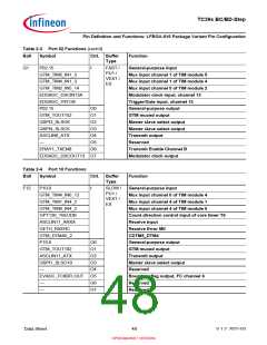
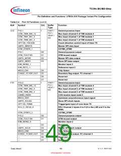
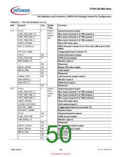
Table 2-4 Port 10 Functions (cont’d)
Ball
Symbol
Ctrl. Buffer
Type
Function
G12
P10.1
I
FAST /
PU1 /
VEXT /
ES
General-purpose input
GTM_TIM4_IN4_12
GTM_TIM1_IN1_3
GTM_TIM0_IN1_3
GPT120_T5EUDB
QSPI1_MRSTA
GTM_DTMT0_1
P10.1
Mux input channel 4 of TIM module 4
Mux input channel 1 of TIM module 1
Mux input channel 1 of TIM module 0
Count direction control input of timer T5
Master SPI data input
CDTM0_DTM0
O0
O1
O2
O3
General-purpose output
GTM muxed output
GTM_TOUT103
QSPI1_MTSR
QSPI1_MRST
IOM_MON2_1
IOM_REF2_1
MSC0_EN1
Master SPI data output
Slave SPI data output
Monitor input 2
Reference input 2
O4
O5
O6
O7
I
Chip Select
EVADC_FC1BFLOUT
—
Boundary flag output, FC channel 1
Reserved
—
Reserved
F10
P10.2
FAST /
PU1 /
VEXT /
ES
General-purpose input
GTM_TIM4_IN5_12
GTM_TIM1_IN2_3
GTM_TIM0_IN2_3
CAN02_RXDE
MSC0_SDI1
Mux input channel 5 of TIM module 4
Mux input channel 2 of TIM module 1
Mux input channel 2 of TIM module 0
CAN receive input node 2
Upstream assynchronous input signal
Slave SPI clock inputs
QSPI1_SCLKA
GPT120_T6INB
SCU_E_REQ2_0
Trigger/gate input of core timer T6
ERU Channel 2 inputs 0 to 5 (0 is the LSB and 5 is the
MSB)
GTM_DTMT2_2
P10.2
CDTM2_DTM0
O0
O1
General-purpose output
GTM muxed output
Monitor input 2
GTM_TOUT104
IOM_MON2_9
—
O2
O3
O4
O5
O6
O7
Reserved
QSPI1_SCLK
MSC0_EN0
EVADC_FC3BFLOUT
—
Master SPI clock output
Chip Select
Boundary flag output, FC channel 3
Reserved
—
Reserved
Data Sheet
49
V 1.2, 2021-03
OPEN MARKET VERSION

 INFINEON [ Infineon ]