TC39x BC/BD-Step
Electrical SpecificationPower Supply Infrastructure and Supply Start-up
basic supply and clock infrastructure is available. During reset release at T3, the load jump of upto 150 mA
(dIDD) is expected.
•
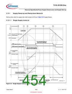
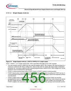
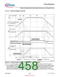
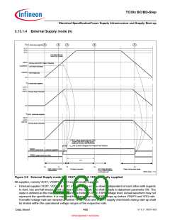
The power sequence as shown in Figure 3-4 is enumerated below
–
T1 up to T2 refers to the period in time when basic supply and clock infrastructure components are
available as the external supply ramps up. The bandgap and internal clock sources are started .The supply
mode is evaluated based on the HWCFG[2:1,4,5,6] and TESTMODE pins. T1 up to T2 refers to the period
in time when basic supply and clock infrastructure components are available as the external supply ramps
up. The bandgap and internal clock sources are started .The supply mode is evaluated based on the
HWCFG[2:1,6] pins. These events are initiated after LVD reset release at T1. LVD reset is released the
both input voltages VEXT and VEVRSB are above VLVDRST5 and VLVDRSTSB levels correspondingly.
Internal pre-regulator VDDPD output voltage is above VLVDRSTC level.
–
–
T2 refers to the point in time where consequently a soft start of EVRC regulator is initiated. PORST (input)
does not have any affect on EVRC output and regulators continue to generate the respective voltages
though PORST is asserted and the device is in reset state. The generated voltage follows a soft ramp-up
over the tSTR (datasheet parameter) time to avoid overshoots.
T3 refers to the point in time when all supplies are above their primary reset thresholds denoted by VRST5,
VRST33 and VRSTC supply voltage levels. EVRC regulator has ramped up. PORST (output) is de-
asserted and HWCFG[3:5] pins are latched on PORST rising edge by SCU. Firmware execution is initiated.
The time between T1 and T3 is documented as tEVRstartup (datasheet parameter).
–
–
T4 refers to the point in time when Firmware execution is completed and User code execution starts with
CPU0 at a default frequency of 100 MHz. The time between T0 and T4 is documented as tBP (datasheet
parameter).
T5 refers to the point in time during the ramp-down phase when at least one of the externally provided or
generated supplies (VDD, VDDP3 or VEXT) drop below their respective primary under-voltage reset
thresholds.
Data Sheet
457
V 1.2, 2021-03
OPEN MARKET VERSION

 INFINEON [ Infineon ]