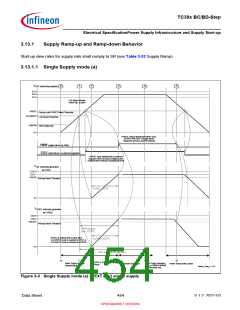
TC39x BC/BD-Step
Electrical SpecificationPower Supply Current
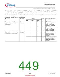
Table 3-28 Module Current Consumption (cont’d)
Parameter
Symbol
Values
Typ.
Unit
Note / Test Condition
Min.
Max.
∑ Sum of external IDDM supply
currents (incl.
I
DDM CC
-
-
44
mA
real power pattern;
current for EDSADC
modules only and
EVADC modules are
inactive; 11 EDSADC
channels active
I
DDMEVADC+IDDMEDSADC)
continuously.
-
-
63 4)
mA
max power pattern;
current for EDSADC
modules only and
EVADC modules are
inactive; all EDSADC
channels active
continuously.
-
-
-
-
16 5)
mA
mA
real power pattern;
current for EVADC
modules only and
EDSADC modules are
inactive; 12 EVADC
modules active.
20 6)
max power pattern;
current for EVADC
modules only and
EDSADC modules are
inactive; all EVADC
modules active.
I
DDP3 supply current for erasing IDDP3ERASE
-
-
-
-
25
mA
mA
Pflash 3.3V erasing
current adder when
using external 3.3V
supply.
of a Pflash or Dflash bank
CC
SCR 8-bit Standby Controller
current incl. PMS in STANDBY
Mode drawn at VEVRSB supply
pin
I
SCRSB CC
7.5 7)
SCR power pattern incl.
PMS current
consumption with fback
clock active; fSYS_SCR
20MHz; TJ=150°C
=
-
-
0.150
-
mA
mA
SCR power pattern incl.
PMS current
consumption with fback
inactive; fSYS_SCR =
70kHz; TJ=25°C
SCR 8-bit Standby Controller
CPU in IDLE mode 8)
I
SCRIDLE CC
-
3.5
real power pattern.
CPU set into idle mode.
1) The same current limits apply also for the other power pattern.
2) During Pflash programming at 5V, additional 3 mA is drawn at VEXT supply rail.
3) A single LVDS pair with receive function is limited to 1.5mA (tEXTLVDS).
Data Sheet
450
V 1.2, 2021-03
OPEN MARKET VERSION

 INFINEON [ Infineon ]