TC39x BC/BD-Step
Electrical SpecificationPower Supply Current
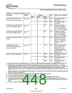
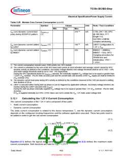
Table 3-27 Current Consumption (cont’d)
Parameter
Symbol
Values
Typ.
Unit
Note / Test Condition
Min.
Max.
∑ Sum of all currents (incl.
I
DDTOT CC
-
-
-
-
1536
mA
mA
mA
real power pattern;
TJ=150°C
I
EXTRAIL+IDDMRAIL+IDDx3RAIL+IDD)
-
-
1720
980
real power pattern;
TJ=160°C
∑ Sum of all currents with DC- IDDTOTDC3
DC EVRC regulator active
real power pattern;
EVRC reset settings
with 72% efficiency;
6)
CC
VEXT = 3.3V; TJ=160°C
∑ Sum of all currents with DC- IDDTOTDC5
-
-
-
-
670
38
mA
mA
real power pattern;
EVRC reset settings
with 72% efficiency;
6)
DC EVRC regulator active
CC
VEXT = 5V; TJ=160°C
∑ Sum of all currents (SLEEP
mode) 1)
I
I
SLEEP CC
All CPUs in idle, All
peripherals in sleep,
fSRI/SPB = 1 MHz via
LPDIV divider; TJ =
25°C
∑ Sum of all currents
STANDBY CC -
-
130 8)
µA
32 kB Standby RAM
block active. SCR
inactive. Power to
(STANDBY mode) drawn at
V
EVRSB supply pin 7)
remaining domains
switched off. TJ = 25°C;
VEVRSB = 5V
Maximum power dissipation 9)
PD SR
-
-
-
-
-
-
2240
3220
2500
mW
mW
mW
ADAS power pattern;
TJ=125°C
max power pattern;
TJ=150°C
real power pattern;
TJ=150°C
1) Limits are defined for real power pattern (VDD=1.275V). For max power pattern limit has to be multiplied by the factor 1.22.
2) Realistic Pflash read pattern with 50% Pflash bandwidth utlilization and a code mix of 50% 0s and 50% 1s. A common
decoupling capacitor of atleast 100nF for (VDDP3) is used. Continuous Dflash programming in burst mode with 3.3 V supply and
realistic Pflash read access in parallel. Erase currents of the corresponding flash modules are less than the respective
programming currents at VDDP3 pin. Programming and erasing flash may generate transient current spikes of up to 45 mA / 20
ns
which are handled by the decoupling and buffer capacitors. This parameter is relevant for external power supply dimensioning
and not for thermal considerations.
3) Limits are defined for real power pattern. For ADAS power pattern limit sum up to 40mA.
4) The current consumption includes only minimal port activity.
5) Limits are defined for real power pattern. For ADAS power pattern limit has to be multiplied by the factor 0.7.
6) The total current drawn from external regulator is estimated with 72% EVRC SMPS regulator efficiency. IDDTOTDCx is
calculated from IDDTOT using the scaled core current [(IDD x VDD)/(VinxEfficiency)] and constitutes all other rail currents and
IDDM.
7) The same current limits apply also for the other power pattern.
Data Sheet
448
V 1.2, 2021-03
OPEN MARKET VERSION

 INFINEON [ Infineon ]