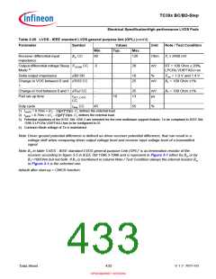
TC39x BC/BD-Step
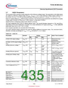
Electrical SpecificationVADC Parameters
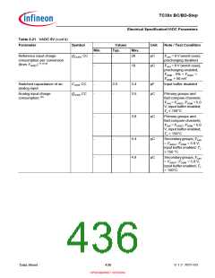
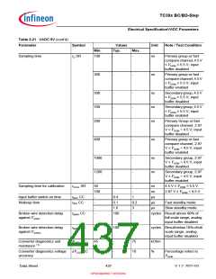
Table 3-21 VADC 5V (cont’d)
Parameter
Symbol
Values
Typ.
Unit
Note / Test Condition
Min.
Max.
Sampling time
tS SR
100
-
-
ns
Primary group or fast
compare channel, 4.5 V
≤ VDDM ≤ 5.5 V; input
buffer disabled
300
-
-
ns
Primary group or fast
compare channel, 4.5 V
≤ VDDM ≤ 5.5 V; input
buffer enabled
500
700
200
-
-
-
-
-
-
ns
ns
ns
Secondary group, 4.5 V
≤ VDDM ≤ 5.5 V; input
buffer disabled
Secondary group, 4.5 V
≤ VDDM ≤ 5.5 V; input
buffer enabled
Primary Group or fast
compare channel, 2.97
V ≤ VDDM < 4.5 V; input
buffer disabled
400
-
-
ns
Primary group or fast
compare channel, 2.97
V ≤ VDDM < 4.5 V; input
buffer enabled
1000
1200
-
-
-
-
ns
ns
Secondary group, 2.97
V ≤ VDDM < 4.5 V; input
buffer disabled
Secondary group, 2.97
V ≤ VDDM < 4.5 V; input
buffer enabled
Sampling time for calibration
t
SCAL SR
50
-
-
ns
ns
µs
µs
µs
4.5 V ≤ VDDM ≤ 5.5 V
2.97 V ≤ VDDM < 4.5 V
100
-
-
Input buffer switch-on time
Wakeup time
t
t
BUF CC
WU CC
-
-
-
-
0.4
0.1
1.6
100
1
0.2
3
-
Fast standby mode
Slow standby mode
Broken wire detection delay
against VAREF
t
t
BWR CC
cycles Result above 80% of
full scale range, analog
input buffer disabled
Broken wire detection delay
against VAGND
BWG CC
-
100
-
cycles Result below 10% of full
scale range, analog
input buffer disabled
Converter diagnostics unit
resistance 11)
R
CSD CC
45
-
-
75
10
kOhm
Converter diagnostics voltage
accuracy
dVCSD CC
-10
%
Percentage refers to
VDDM
Data Sheet
437
V 1.2, 2021-03
OPEN MARKET VERSION

 INFINEON [ Infineon ]