TC39x BC/BD-Step
Electrical SpecificationHigh performance LVDS Pads
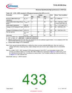
Table 3-20 LVDS - IEEE standard LVDS general purpose link (GPL) (cont’d)
Parameter
Symbol
Values
Typ.
Unit
Note / Test Condition
Min.
Max.
Receiver differential input
impedance
Rin CC
80
-
120
Ohm
mV
VI ≤ 2400 mV
Output differential voltage Sleep VODSM CC
-5
-
20
RT = 100 Ohm ± 20%;
LPCRx.VDIFFADJ=xx
Mode 4)
Delta output impedance
dR0 SR
-
-
-
-
10
25
%
Vcm = 1.0 V and 1.4 V
Change in VOS between 0 and dVOS CC
mV
RT = 100 Ohm ±1%
1
Change in Vod between 0 and 1 dVod CC
-
-
-
25
13
mV
µs
RT = 100 Ohm ±1%
Pad set-up time
tSET_LVDS
10
CC
Duty cycle
t
duty CC
45
-
55
%
1) trise20 = 0.75ns + (CL - 2)[pF]*20ps. CL defines the external load.
2) tfall20 = 0.75ns + (CL - 2)[pF]*20ps. CL defines the external load.
3) Potential violations of the IEEE Std 1596.3 are intended for the new multislave support feature. To be compliant to IEEE Std
1596.3 LPCRx.VDIFFADJ has to be configured to 01.
4) Common Mode voltage of Tx is maintained.
Note:Driver ground potential difference is defined as driver-receiver potentital difference, that can result in a
voltage shift when comparing driver output voltage level and receiver input voltage level of a transmitted
signal.
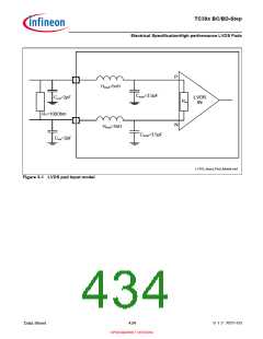
Note:RT in table ‘LVDS - IEEE standard LVDS general purpose Link (GPL)’ is as termination resistor of the
receiver according to figure 3-5 in IEEE Std 1596.3-1996 and is represent in Figure 3-1 either by Rin or by
RT=100Ohm but not both. If RT is mentioned in column Note / Test Condition always the internal resistor Rin
in Figure 3-1 is the selected one.
default after start-up = CMOS function
Data Sheet
433
V 1.2, 2021-03
OPEN MARKET VERSION

 INFINEON [ Infineon ]