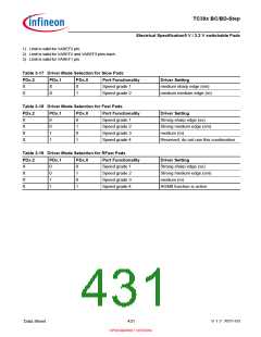
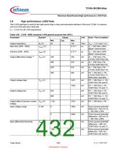
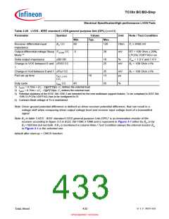
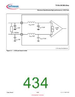
TC39x BC/BD-Step
Electrical SpecificationVADC Parameters
3.7
VADC Parameters
The accuracy of the converter results depends on the reference voltage range. The parameters in the table below
are valid for a reference voltage range of (VAREF - VAGND) >= 4.5 V. If the reference voltage range is below 4.5 V
by a factor of k (e.g. 3.3 V), the accuracy parameters increase by a factor of 1.1/k (e.g. 1.1 × 4.5 / 3.3 = 1.5).
Noise on supply voltage VDDM influences the conversion. The accuracy (error) parameters are defined for a supply
voltage ripple of below 20 mVpp up to 10 MHz (below 5 mVpp above 10 MHz).
Digital functions overlapping analog inputs influence accuracy.
The total unadjusted error (TUE) is defined without noise. The overall deviation depends on TUE and ENRMS
(depending on the noise distribution). Example: For a noise distribution of 4 sigma and ENRMS = 1.0 the additional
peak-peak noise error is ±(4 × 1.0) = 8 LSB12.
Fast compare operations are executed with 10-bit values.
The noise reduction feature improves the result by adding additional conversion steps. The conversion times,
therefore, increase accordingly (4 × tADCI + 3 × tADC for each of 1, 3, or 7 steps).
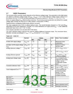
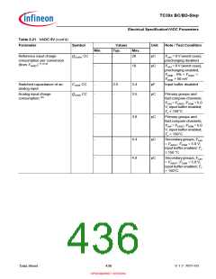
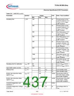
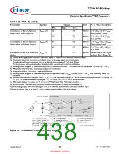
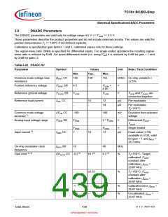
Table 3-21 VADC 5V
Parameter
Symbol
Values
Typ.
Unit
Note / Test Condition
Min.
Max.
EVADC IVR output voltage
V
DDK CC
1.15
-
1.35
V
%
V
V
V
V
Measured at low
temperature.
Deviation of IVR output voltage dVDDK CC
VDDK
Analog reference voltage 1)
-2
-
2
Based on device-
specific value
V
AREF SR
4.5
5.0
3.3
VSSM
-
VDDM
0.05
+
+
4.5 V ≤ VDDM ≤ 5.5 V
2.97
VSSM
VAGND
VDDM
0.05
2.97 V ≤ VDDM < 4.5 V
Analog reference ground
Analog input voltage range
V
V
AGND SR
AIN SR
VSSM
V
SSM and VAGND are
connected together
AIN is limited by the
VAREF
V
respective pad supply
voltage; see pin
configuration (buffer
type)
Converter reference clock
Total Unadjusted Error 2) 3)
f
ADCI SR
16
16
-4
40
20
-
53.33
26.67
4
MHz
MHz
LSB
4.5 V ≤ VDDM ≤ 5.5 V
2.97 V ≤ VDDM < 4.5 V
TUE CC
12-bit resolution for
primary/secondary
groups, 10-bit
resolution for fast
compare channels
INL Error 2)
DNL error 2)4)
Gain Error 2)
Offset Error 2)3)
RMS Noise 2)5) 6)
EAINL CC
EADNL CC
-3
-1
-
3
LSB
LSB
LSB
LSB
LSB
LSB
-
3
EAGAIN CC -3.5
-
3.5
4
EAOFF CC
ENRMS CC
-4
-
-
0.5
0.5
0.8
1.0
Noise reduction level 3
Standard conversion
-
Data Sheet
435
V 1.2, 2021-03
OPEN MARKET VERSION

 INFINEON [ Infineon ]