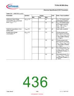
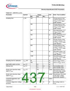
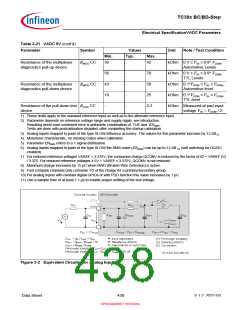
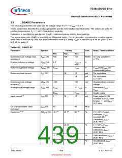
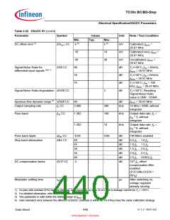
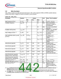
TC39x BC/BD-Step
Electrical SpecificationDSADC Parameters
Table 3-22 DSADC 5V (cont’d)
Parameter
Symbol
Values
Typ.
Unit
Note / Test Condition
Min.
Max.
DC offset error 3)
EDOFF CC -5 5)
-
-
-
-
-
-
-
5 5)
mV
mV
mV
dB
dB
dB
dB
Calibrated; fMOD =
26.67 MHz
-10
-30
10
30
-
Calibrated once; fMOD =
26.67 MHz
Uncalibrated; fMOD
26.67 MHz
=
Signal-Noise Ratio for
differential input signals 2)6) 7)
SNR CC
80
78
74
-
TJ≤150°C; fPB = 30 kHz;
MOD = 26.67 MHz
TJ≤150°C; fPB = 50 kHz;
MOD = 26.67 MHz
f
-
f
-
TJ≤150°C; fPB = 100
kHz; fMOD = 26.67 MHz
Signal-Noise Ratio degradation DSNR CC
Spurious-free dynamic range 3) SFDR CC
3
TJ>150°C; Resulting
Signal-Noise Ratio
value is SNR - DSNR
60
-
-
-
dB
fMOD = 26.67 MHz
Output sampling rate
fD CC
3.906
300
kHz
16 MHz / 4096, without
integrator
Pass band
f
PB CC
1.302
1.302
-
-
100
10
kHz
kHz
Output data rate: fD =
fPB * 3; without
integrator
Output data rate: fD =
fPB * 6; without
integrator
Pass band ripple
dfPB CC
SBA CC
-0.08
40
-
-
-
-
-
-
-
0.08
dB
dB
dB
dB
dB
dB
dB
FIR filters enabled
0.5 fD ... 1.0 fD
1.0 fD ... 1.5 fD
1.5 fD ... 2.0 fD
2.0 fD ... 2.5 fD
2.5 fD ... OSR/2 fD
10-5 fD, offset
compensation filter
enabled
Stop band attenuation
-
-
-
-
-
-
45
50
55
60
DC compensation factor
Modulator settling time
DCF CC
-3
(FCFGMx.OCEN =
001B)
t
MSET CC
-
-
20
µs
After switching on,
voltage regulator
already running
1) On pins with overlaid GPIO function the max. limit increases by up to 25 mV due to leakage current for TJ > 150°C.
2) For detailed information, refer to the User Manual chapter.
3) This parameter is valid within the defined range of fMOD
.
4) Gain mismatch error between the different EDSADC channels is within ±0.5% if they have the same calibration strategy
Data Sheet
440
V 1.2, 2021-03
OPEN MARKET VERSION

 INFINEON [ Infineon ]