TC39x BC/BD-Step
Electrical SpecificationDSADC Parameters
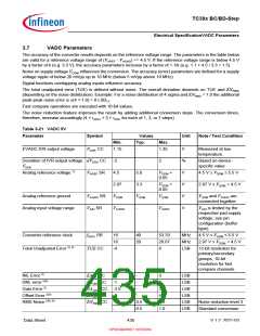
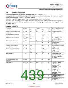
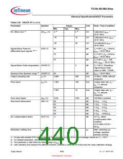
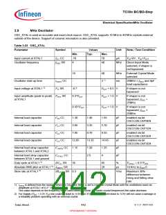
3.8
DSADC Parameters
The DSADC parameters are valid only for voltage range 4.5 V <= VDDM <= 5.5 V.
These parameters describe the product properties and do not include external circuitry. The values are valid for
junction temperatures TJ <= 150°C if not defined explicitly.
Calibration is specified for gain factors 1 and 2, calibrated values refer to these settings.
The signal-noise ratio (SNR) is specified for differential inputs. For single ended operation the resulting signal-
noise ratio is reduced by 6 dB. For quasi-differential mode (i.e. using VCM) it is reduced by 6 dB for gain = 1 and
by 3 dB for gain= 2.
Table 3-22 DSADC 5V
Parameter
Symbol
Values
Typ.
Unit
Note / Test Condition
Min.
Max.
Common mode voltage bias
resistance
R
V
V
BIAS CC
AREF SR
AGND SR
105
130
155
kOhm On-chip variation ≤
±2.5%.
Positive reference voltage
Reference ground voltage
Reference load current
4.5
-
-
VDDM
0.05
+
V
VSSM
VSSM
V
VSSM and VAGND are
connected together
I
REF CC
-
-
10
-
12
14
µA
µA
Per modulator
Per modulator,
TJ>150°C
Common mode voltage
accuracy 1)
dVCM CC
DSIN SR
-100
-
-
100
mV
V
Deviation from selected
voltage
Analog input voltage range
V
VSSM
2 * VDDM
Differential;VDSxP -
VDSxN
VSSM
-
VDDM
V
Single ended
Input current 2)
I
RMS CC
7
10
13
µA
Exact value (±1%)
available in UCB; valid
for gain = 1 and fMOD
=
26.7 MHz
On-chip modulator clock
frequency
Gain error 3) 4)
f
MOD SR
16
-
40
MHz
%
EDGAIN CC -0.2 5)
±0.15)
0.2 5)
TJ≤150°C; Target,
calibrated, VAREF
constant after
calibration; fMOD
=
26.67 MHz
-
±0.25
-
%
TJ>150°C; VAREF
constant after
calibration; fMOD
=
26.67 MHz
-1
-
-
1
%
%
Calibrated once; fMOD =
26.67 MHz
-2.5
2.5
Uncalibrated; fMOD =
26.67 MHz
Data Sheet
439
V 1.2, 2021-03
OPEN MARKET VERSION

 INFINEON [ Infineon ]