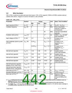
TC39x BC/BD-Step
Electrical SpecificationVADC Parameters
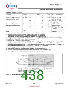
Table 3-21 VADC 5V (cont’d)
Parameter
Symbol
Values
Typ.
Unit
Note / Test Condition
Min.
Max.
Resistance of the multiplexer
diagnostics pull-up device
R
MDU CC
30
-
-
-
-
-
42
kOhm 0 V ≤ VIN ≤ 0.9* VDDM
,
,
Automotive Levels
56
43
18
-
78
58
25
0.3
kOhm 0 V ≤ VIN ≤ 0.9* VDDM
TTL Levels
Resistance of the multiplexer
diagnostics pull-down device
R
MDD CC
kOhm 0.1*VDDM ≤ VIN ≤ VDDM
,
Automotive level
kOhm 0.1*VDDM ≤ VIN ≤ VDDM
,
TTL level
Resistance of the pull-down test RPDD CC
kOhm Measured at pad input
device
voltage VIN = VDDM / 2.
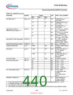
1) These limits apply to the standard reference input as well as to the alternate reference input.
2) Parameter depends on reference voltage range and supply ripple, see introduction.
Resulting worst case combined error is arithmetic combination of TUE and ENRMS
.
Tests are done with postcalibration disabled, after completing the startup calibration.
3) Analog inputs mapped to pads of the type SLOW influence accuracy. The values for this parameter increase by 3 LSB12.
4) Monotonic characteristic, no missing codes when calibrated.
5) Parameter ENRMS refers to a 1 sigma distribution.
6) Analog inputs mapped to pads of the type SLOW the RMS noise (ENRMS) can be up to 2 LSB 12 (soft switching for DC/DC
enabled).
7) For reduced reference voltages VAREF < 3.375V, the consumed charge QCONV is reduced by the factor of k2 = VAREF [V]
/ 3.375. For reduced reference voltages 4.5V < VAREF ≤ 3.375V, QCONV is not reduced.
8) Maximum charge increases by 15 pC when BWD (Broken Wire Detection) is active.
9) Fast compare channels only consume 1/3 of the charge for a primary/secondary group.
10) For analog inputs with overlaid digital GPIOs or with PDD function this value increases by 1 pC.
11) Use a sample time of at least 1.1 µs to enable proper settling of the test voltage.
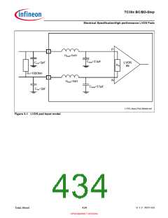
Figure 3-2 Equivalent Circuitry for Analog Inputs
Data Sheet
438
V 1.2, 2021-03
OPEN MARKET VERSION

 INFINEON [ Infineon ]