TC39x BC/BD-Step
Electrical SpecificationHigh performance LVDS Pads
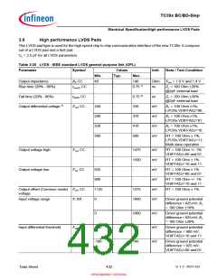
3.6
High performance LVDS Pads
This LVDS pad type is used for the high speed chip to chip communication interface of the new TC39x. It compose
out of a LVDS pad and a fast pad.
CL = 2.5 pF for all LVDS parameters.
Table 3-20 LVDS - IEEE standard LVDS general purpose link (GPL)
Parameter
Symbol
Values
Typ.
Unit
Note / Test Condition
Min.
40
-
Max.
140
0.75 1)
Output impedance
R0 CC
-
-
Ohm
ns
Vcm = 1.0 V and 1.4 V
Rise time (20% - 80%)
t
rise20 CC
ZL = 100 Ohm ±20%
@2pF external load
Fall time (20% - 80%)
t
fall20 CC
-
-
-
-
-
-
0.75 2)
330
ns
ZL = 100 Ohm ±20%
@2pF external load
Output differential voltage 3)
V
OD CC
240
280
320
380
mV
mV
mV
mV
RT = 100 Ohm ±1%;
LPCRx.VDIFFADJ=00
370
RT = 100 Ohm ±1%;
LPCRx.VDIFFADJ=01
410
RT = 100 Ohm ±1%;
LPCRx.VDIFFADJ=10
500
RT = 100 Ohm ± 1%;
LPCRx.VDIFFADJ=11;
Multi slave operation
Output voltage high
Output voltage low
V
V
V
OH CC
OL CC
OS CC
-
-
-
-
-
-
-
1475
1500
-
mV
mV
mV
mV
mV
mV
RT = 100 Ohm +/- 1%
VDIFFADJ=00 and 01
-
RT = 100 Ohm ± 1%
VDIFFADJ=10 and 11
925
900
1125
0
RT = 100 Ohm ± 1%
VDIFFADJ=00 and 01
-
RT = 100 Ohm +/- 1%
VDIFFADJ=10 and 11
Output offset (Common mode)
voltage
1275
1600
RT = 100 Ohm ± 1%
Input voltage range
VI SR
Driver ground potential
difference < 925 mV; RT
= 100 Ohm ±10%
0
-
-
-
2400
100
mV
mV
mV
Driver ground potential
difference < 925 mV; RT
= 100 Ohm ±20%
Input differential threshold
V
idth SR
-100
-100
Driver ground potential
difference < 900 mV;
VDIFFADJ=10 and 11
100
Driver ground potential
difference < 925 mV;
VDIFFADJ=00 and 01
Data Sheet
432
V 1.2, 2021-03
OPEN MARKET VERSION

 INFINEON [ Infineon ]