TC39x BC/BD-Step
Electrical Specification5 V / 3.3 V switchable Pads
3.5
5 V / 3.3 V switchable Pads
Pad classes slow GPIO and fast GPIO support both Automotive Level (AL) or TTL level (TTL) operation.
Parameters are defined for AL operation and degrade in TTL operation.
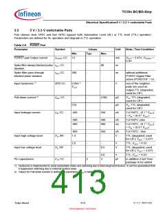
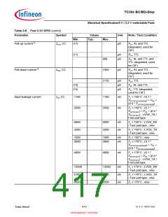
Table 3-6 PORST Pad
Parameter
Symbol
Values
Typ.
Unit
Note / Test Condition
Min.
Max.
PORST pad Output current
I
PORST CC
13
-
-
-
-
mA
ns
VEXT = 2.97V; VPORST =
0.9V
Spike filter always blocked pulse tSF1 CC
duration
-
80
-
Spike filter pass-through
blocked pulse duration
t
SF2 CC
260
ns
without additional
PORST Digtial Filter
active (PORSTDF = 0).
Input hysteresis 1)
HYS CC
0.055 *
VEXT
-
-
V
non of the neighbor
pads are used as
output;TTL (degraded,
used for CIF)
Pull-down current 2)
I
I
PDL CC
-
-
-
-
|130|
-
µA
µA
nA
VIH; TTL (degraded,
used for CIF)
|15|
-450
VIL; TTL (degraded,
used for CIF)
Input leakage current
OZ CC
450
TJ≤150°C ; (0.1 * VEXT
)
)
< VIN < (0.9 * VEXT
)
-500
-900
-
-
500
900
nA
nA
TJ≤150°C ;else
TJ≤170°C ; (0.1 * VEXT
< VIN < (0.9 * VEXT
)
-950
1.4
-
-
950
-
nA
V
TJ≤170°C ; else
Input high voltage level
Input low voltage level
Pin capacitance
VIH SR
VIL SR
CIO CC
TTL (degraded, used
for CIF); VEXT = 2.97V
2.0
-
-
-
-
V
V
TTL; VEXT = 4.5V
0.5
TTL (degraded, used
for CIF); VEXT = 2.97V
-
-
-
0.8
3
V
TTL; VEXT = 4.5V
2
pF
in addition 2.5pF from
package to be added
1) Hysteresis is implemented to avoid metastable states and switching due to internal ground bounce. It can't be guaranteed that
it suppresses switching due to external system noise.
2) Values for Pull-down resistor is defined via parameter RMDD in table VADC 5V.
Data Sheet
413
V 1.2, 2021-03
OPEN MARKET VERSION

 INFINEON [ Infineon ]