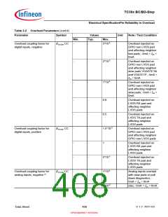
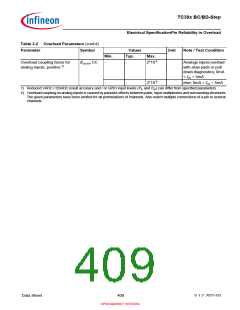
TC39x BC/BD-Step
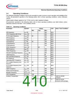
Electrical SpecificationOperating Conditions
Table 3-3 Operating Conditions (cont’d)
Parameter
Symbol
Values
Typ.
Unit
Note / Test Condition
Min.
Max.
0.1
Analog ground voltage for VDDM
V
V
SSM CC
EVRSB SR 2.97 5)
-0.1
0
-
V
V
Digital external supply voltage
for EVR and during Standby
mode
5.5
Voltage to ensure defined pad
states
V
DDPPA CC 1.3 6)
-
-
V
1) For VDD 1.08V ≤ VDD < 1.125V operation is still possible but with relaxed parameters.
2) Voltage overshoot to 1.69V is permissible, provided the duration is less than 2h cumulated. Reduced ADC accuracy and
leakage is increased.
3) Voltage overshoot to 6.5V is permissible, provided the duration is less than 2h cumulated. Reduced ADC accuracy and
leakage is increased.
4) Voltage overshoot to 4.29V is permissible, provided the duration is less than 2h cumulated. Reduced ADC accuracy and
leakage is increased.
5) VEVRSB supply voltage can drop down upto 2.6V during Standby mode. It is required to have a capictor of 100nF on VEVRSB
supply pin.
6) HWCFG[6] pin is latched and pull-up or tristate is activated at Port pins when VEXT has reached this level.
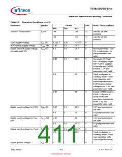
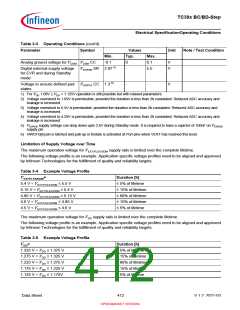
Limitation of Supply Voltage over Time
The maximum operation voltage for VEXT/FLEX/DDM supply rails is limited over the complete lifetime.
The following voltage profile is an example. Application specific voltage profiles need to be aligned and approved
by Infineon Technologies for the fulfillment of quality and reliability targets.
Table 3-4 Example Voltage Profile
VEXT/FLEX/DDM
=
Duration [h]
5.4 V < VEXT/FLEX/DDM ≤ 5.5 V
5.15 V < VEXT/FLEX/DDM ≤ 5.4 V
4.85 V < VEXT/FLEX/DDM ≤ 5.15 V
4.6 V < VEXT/FLEX/DDM ≤ 4.85 V
4.5 V < VEXT/FLEX/DDM ≤ 4.6 V
≤ 5% of lifetime
≤ 15% of lifetime
≤ 60% of lifetime
≤ 15% of lifetime
≤ 5% of lifetime
The maximum operation voltage for VDD supply rails is limited over the complete lifetime.
The following voltage profile is an example. Application specific voltage profiles need to be aligned and approved
by Infineon Technologies for the fulfillment of quality and reliability targets.
Table 3-5 Example Voltage Profile
VDD=
Duration [h]
1.325 V < VDD ≤ 1.375 V
1.275 V < VDD ≤ 1.325 V
1.225 V < VDD ≤ 1.275 V
1.175 V < VDD ≤ 1.225 V
1.125 V < VDD ≤ 1.175V
≤ 5% of lifetime
≤ 15% of lifetime
≤ 60% of lifetime
≤ 15% of lifetime
≤ 5% of lifetime
Data Sheet
412
V 1.2, 2021-03
OPEN MARKET VERSION

 INFINEON [ Infineon ]