TC39x BC/BD-Step
Electrical Specification5 V / 3.3 V switchable Pads
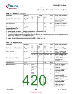
3) Hysteresis is implemented to avoid metastable states and switching due to internal ground bounce. It can't be guaranteed that
it suppresses switching due to external system noise.
4) Values for Pull-up resistor is defined via parameter RMDU in table VADC 5V.
5) Values for Pull-down resistor is defined via parameter RMDD in table VADC 5V.
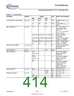
Table 3-8 Fast 3.3V GPIO
Parameter
Symbol
Values
Typ.
Unit
Note / Test Condition
Min.
Max.
On-Resistance of pad output
R
DSON CC
125
225
55
-
320
Ohm
Ohm
ns
medium driver; IOH / OL =
2mA
31
80
strong driver; IOH / OL =
8mA
Rise / Fall time 1) 2)
t
RF CC
1.6
4.5
CL = 25pF; driver =
strong sharp edge;
from 0.2 *
VEXT/FLEX/EVRSB to 0.8 *
VEXT/FLEX/EVRSB
-
-
5
ns
CL = 25pF; driver =
strong sharp edge;
from 0.8V to 2.0V
(RMII)
2+0.57*CL 5.5+0.75* 10+1.25* ns
CL CL
1.5+0.18* 1.5+0.28* 8+0.4*CL ns
CL CL
driver = medium;
CL≤200pF
driver = strong edge =
medium; CL≤200pF
0.75+0.08 0.75+0.11 2.5+0.21* ns
driver = strong edge =
*CL
*CL
CL
sharp ; CL≤200pF
Asymmetry of sending
t
TX_ASYM CC -1
-
1
ns
valid for all data rates
excluding clock
tolerance
Input frequency
Input hysteresis 3)
fIN CC
-
-
-
160
-
MHz
V
HYS CC
0.055 *
non of the neighbor
pads are used as
output; AL
VEXT/FLEX/E
VRSB
0.09 *
VEXT/FLEX/E
-
-
-
-
V
V
non of the neighbor
pads are used as
output; TTL
VRSB
0.055 *
VEXT/FLEX/E
non of the neighbor
pads are used as
output;TTL (degraded,
used for CIF)
VRSB
125
-
-
mV
two of the neighbor
pads are used as
output with
driver=strong and
edge=sharp; AL
Data Sheet
416
V 1.2, 2021-03
OPEN MARKET VERSION

 INFINEON [ Infineon ]