TC1767
Electrical Parameters
7) The RCLK max. input rise/fall times are best case parameters for fSYS = 80 MHz. For reduction of EMI, slower
input signal rise/fall times can be used for longer RCLK clock periods.
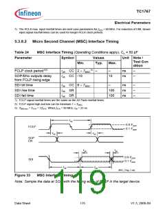
5.3.8.2 Micro Second Channel (MSC) Interface Timing
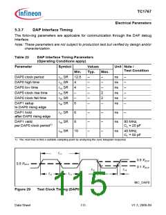
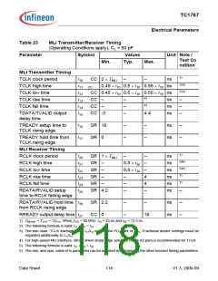
Table 24
MSC Interface Timing (Operating Conditions apply), CL = 50 pF
Parameter
Symbol
Values
Typ.
Unit Note /
Test Con
Min.
Max.
dition
FCLP clock period1)2)
t40 CC 2 × TMSC
t45 CC -10
–
–
ns
ns
–
–
3)
SOP/ENx outputs delay
from FCLP rising edge
10
SDI bit time
SDI rise time
SDI fall time
t46 CC 8 × TMSC
t48 SR
–
ns
ns
ns
–
–
–
100
100
t49 SR
1) FCLP signal rise/fall times are the same as the A2 Pads rise/fall times.
2) FCLP signal high and low can be minimum 1 × TMSC
.
3) TMSCmin = TSYS = 1/fSYS. When fSYS = 80 MHz, t40 = 25 ns
t40
0.9 VDDP
0.1 VDDP
FCLP
t45
t45
SOP
EN
t48
t49
0.9 VDDP
0.1 VDDP
SDI
t46
t46
MSC_Tmg_1.vsd
Figure 33
MSC Interface Timing
Note: Sample the data at SOP with the falling edge of FCLP in the target device.
Data Sheet
115
V1.3, 2009-09

 INFINEON [ Infineon ]