TC1767
Electrical Parameters
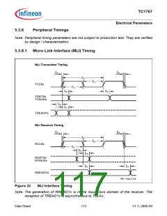
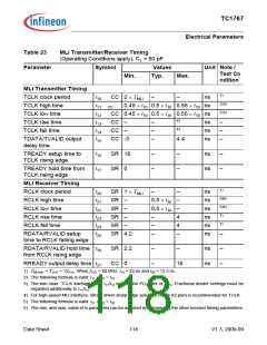
Table 23
MLI Transmitter/Receiver Timing
(Operating Conditions apply), CL = 50 pF
Parameter
Symbol
Values
Unit Note /
Test Co
Min.
Typ.
Max.
ndition
MLI Transmitter Timing
TCLK clock period
TCLK high time
1)
t10
t11
t12
t13
t14
t15
CC 2 × TMLI
–
–
ns
2)3)
2)3)
0.45 × t10 0.5 × t10 0.55 × t10 ns
CC
TCLK low time
CC 0.45 × t10 0.5 × t10 0.55 × t10 ns
4)
TCLK rise time
CC –
CC –
CC -3
–
–
–
ns
ns
ns
–
–
–
4)
TCLK fall time
TDATA/TVALID output
delay time
4.4
TREADY setup time to
TCLK rising edge
t16
t17
SR 18
SR 0
–
–
–
–
ns
ns
–
–
TREADY hold time from
TCLK rising edge
MLI Receiver Timing
RCLK clock period
RCLK high time
RCLK low time
1)
t20
t21
t22
t23
t24
t25
SR 1 × TMLI
SR –
–
–
–
–
4
4
–
ns
ns
ns
ns
ns
ns
5)6)
5)6)
7)
0.5 × t20
SR –
0.5 × t20
RCLK rise time
SR –
–
–
–
7)
RCLK fall time
SR –
RDATA/RVALID setup
time to RCLK falling edge
SR 4.2
–
–
–
RDATA/RVALID hold time t26
from RCLK rising edge
SR 2.2
–
–
ns
ns
RREADY output delay time t27
CC 0
–
16
1) TMLImin. = TSYS = 1/fSYS. When fSYS = 80 MHz, t10 = 25 ns and t20 = 12.5 ns.
2) The following formula is valid: t11 + t12 = t10
3) The min./max. TCLK low/high times t11/t12 include the PLL jitter of fSYS. Fractional divider settings must be
regarded additionally to t11/t12.
4) For high-speed MLI interface, strong driver sharp edge selection (class A2 pad) is recommended for TCLK.
5) The following formula is valid: t21 + t22 = t20
6) The min. and max. value of is parameter can be adjusted by considering the other receiver timing parameters.
Data Sheet
114
V1.3, 2009-09

 INFINEON [ Infineon ]