C167CR
C167SR
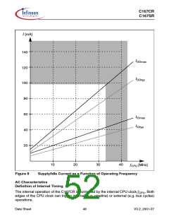
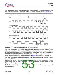
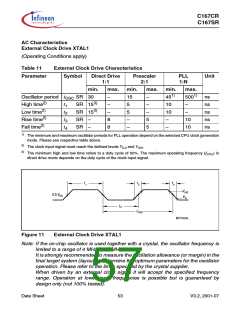
The specification of the external timing (AC Characteristics) therefore depends on the
time between two consecutive edges of the CPU clock, called “TCL” (see Figure 9).
Phase Locked Loop Operation
fOSC
TCL
fCPU
TCL
Direct Clock Drive
fOSC
TCL
fCPU
TCL
Prescaler Operation
fOSC
TCL
fCPU
MCT04338
TCL
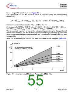
Figure 9
Generation Mechanisms for the CPU Clock
The CPU clock signal fCPU can be generated from the oscillator clock signal fOSC via
different mechanisms. The duration of TCLs and their variation (and also the derived
external timing) depends on the used mechanism to generate fCPU. This influence must
be regarded when calculating the timings for the C167CR.
Note: The example for PLL operation shown in Figure 9 refers to a PLL factor of 4.
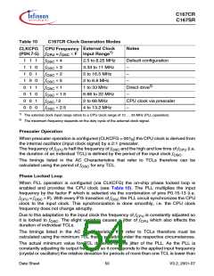
The used mechanism to generate the basic CPU clock is selected by bitfield CLKCFG
in register RP0H.7-5.
Upon a long hardware reset register RP0H is loaded with the logic levels present on the
upper half of PORT0 (P0H), i.e. bitfield CLKCFG represents the logic levels on pins
P0.15-13 (P0H.7-5).
Table 10 associates the combinations of these three bits with the respective clock
generation mode.
Data Sheet
49
V3.2, 2001-07

 INFINEON [ Infineon ]