C167CR
C167SR
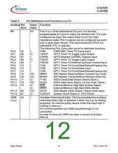
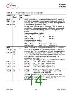
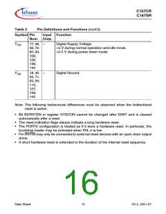
Table 2
Pin Definitions and Functions (cont’d)
Symbol Pin
Input Function
Num. Outp.
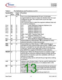
P4
IO
Port 4 is an 8-bit bidirectional I/O port. It is bit-wise
programmable for input or output via direction bits. For a pin
configured as input, the output driver is put into high-
impedance state.
Port 4 can be used to output the segment address lines and
for serial bus interfaces:
P4.0
P4.1
P4.2
P4.3
P4.4
P4.5
85
86
87
88
89
90
O
O
O
O
O
O
I
O
O
O
A16
A17
A18
A19
A20
A21
Least Significant Segment Address Line
Segment Address Line
Segment Address Line
Segment Address Line
Segment Address Line
Segment Address Line,
CAN1_RxD CAN 1 Receive Data Input
A22 Segment Address Line,
CAN1_TxD CAN 1 Transmit Data Output
P4.6
91
P4.7
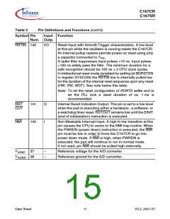
RD
92
95
A23
Most Significant Segment Address Line
O
External Memory Read Strobe. RD is activated for every
external instruction or data read access.
WR/
WRL
96
O
External Memory Write Strobe. In WR-mode this pin is
activated for every external data write access. In WRL-mode
this pin is activated for low byte data write accesses on a
16-bit bus, and for every data write access on an 8-bit bus.
See WRCFG in register SYSCON for mode selection.
READY 97
I
Ready Input. When the Ready function is enabled, a high
level at this pin during an external memory access will force
the insertion of memory cycle time waitstates until the pin
returns to a low level.
An internal pullup device will hold this pin high when nothing
is driving it.
ALE
EA
98
99
O
I
Address Latch Enable Output. Can be used for latching the
address into external memory or an address latch in the
multiplexed bus modes.
External Access Enable pin. A low level at this pin during and
after Reset forces the C167CR to begin instruction execution
out of external memory. A high level forces execution out of
the internal program memory.
“ROMless” versions must have this pin tied to ‘0’.
Data Sheet
9
V3.2, 2001-07

 INFINEON [ Infineon ]