C167CR
C167SR
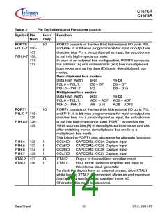
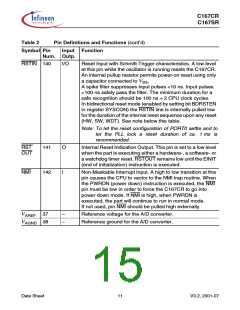
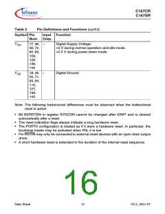
Table 2
Pin Definitions and Functions (cont’d)
Symbol Pin
Input Function
Num. Outp.
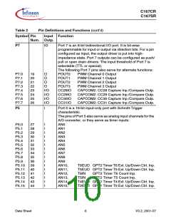
PORT0
P0L.0-7 100-
107
P0H.0-7 108,
111-
IO
PORT0 consists of the two 8-bit bidirectional I/O ports P0L
and P0H. It is bit-wise programmable for input or output via
direction bits. For a pin configured as input, the output driver
is put into high-impedance state.
In case of an external bus configuration, PORT0 serves as
the address (A) and address/data (AD) bus in multiplexed
bus modes and as the data (D) bus in demultiplexed bus
modes.
117
Demultiplexed bus modes:
Data Path Width:
P0L.0 – P0L.7:
P0H.0 – P0H.7:
8-bit
D0 – D7
I/O
16-bit
D0 – D7
D8 – D15
Multiplexed bus modes:
Data Path Width:
P0L.0 – P0L.7:
P0H.0 – P0H.7:
8-bit
16-bit
AD0 – AD7 AD0 – AD7
A8 – A15 AD8 – AD15
PORT1
P1L.0-7 118-
IO
PORT1 consists of the two 8-bit bidirectional I/O ports P1L
and P1H. It is bit-wise programmable for input or output via
direction bits. For a pin configured as input, the output driver
is put into high-impedance state. PORT1 is used as the
16-bit address bus (A) in demultiplexed bus modes and also
after switching from a demultiplexed bus mode to a
multiplexed bus mode.
125
P1H.0-7 128-
135
The following PORT1 pins also serve for alternate functions:
P1H.4 132
P1H.5 133
P1H.6 134
P1H.7 135
I
I
I
I
CC24IO
CC25IO
CC26IO
CC27IO
CAPCOM2: CC24 Capture Input
CAPCOM2: CC25 Capture Input
CAPCOM2: CC26 Capture Input
CAPCOM2: CC27 Capture Input
XTAL2 137
XTAL1 138
O
I
XTAL2:
XTAL1:
Output of the oscillator amplifier circuit.
Input to the oscillator amplifier and input to
the internal clock generator
To clock the device from an external source, drive XTAL1,
while leaving XTAL2 unconnected. Minimum and maximum
high/low and rise/fall times specified in the AC
Characteristics must be observed.
Data Sheet
10
V3.2, 2001-07

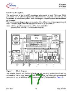
 INFINEON [ Infineon ]