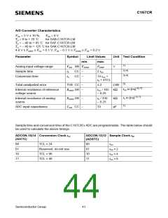
C167CR
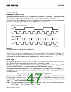
Phase Locked Loop
When pin P0.15 (P0H.7) is high (‘1’) during reset the on-chip phase locked loop is enabled and
provides the CPU clock. The PLL multiplies the input frequency by 4 (i.e. fCPU = fXTAL × 4). With every
fourth transition of fXTAL the PLL circuit synchronizes the CPU clock to the input clock. This
synchronization is done smoothly, i.e. the CPU clock frequency does not change abruptly.
Due to this adaptation to the input clock the frequency of fCPU is constantly adjusted so it is locked
to fXTAL. The slight variation causes a jitter of fCPU which also effects the duration of individual TCLs.
The timings listed in the AC Characteristics that refer to TCLs therefore must be calculated using the
minimum TCL that is possible under the respective circumstances.
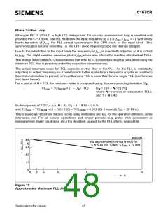
The actual minimum value for TCL depends on the jitter of the PLL. As the PLL is constantly
adjusting its output frequency so it corresponds to the applied input frequency (crystal or oscillator)
the relative deviation for periods of more than one TCL is lower than for one single TCL (see formula
and figure below).
For a period of N × TCL the minimum value is computed using the corresponding deviation D :
N
TCL
= TCL
× (1 – D / 100)
D = ± (4 – N /15) [%],
min
NOM
N
N
where N = number of consecutive TCLs
and 1 ≤ N ≤ 40.
So for a period of 3 TCLs (i.e. N = 3): D = 4 – 3/15 = 3.8 %,
3
and TCL
= TCL
× (1 – 3.8 / 100) = TCL
× 0.962 (24.1 nsec @ fCPU = 20 MHz).
min
NOM
NOM
This is especially important for bus cycles using waitstates and e.g. for the operation of timers, serial
interfaces, etc. For all slower operations and longer periods (e.g. pulse train generation or
measurement, lower baudrates, etc.) the deviation caused by the PLL jitter is neglectible.
Figure 12
Approximated Maximum PLL Jitter
Semiconductor Group
45

 INFINEON [ Infineon ]