C167CR
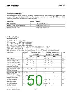
Memory Cycle Variables
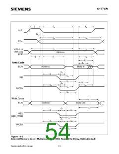
The timing tables below use three variables which are derived from the BUSCONx registers and
represent the special characteristics of the programmed memory cycle. The following table
describes, how these variables are to be computed.
Description
Symbol Values
ALE Extension
tA
tC
tF
TCL × <ALECTL>
Memory Cycle Time Waitstates
Memory Tristate Time
2TCL × (15 – <MCTC>)
2TCL × (1 – <MTTC>)
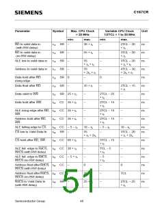
AC Characteristics
Multiplexed Bus
V
CC = 5 V ± 10 %;
VSS = 0 V
for SAB-C167CR-LM
TA = 0 to + 70 ˚C
TA = − 40 to + 85 ˚C for SAF-C167CR-LM
TA = − 40 to + 125 ˚C for SAK-C167CR-LM
CL (for PORT0, PORT1, Port 4, ALE, RD, WR, BHE, CLKOUT) = 100 pF
CL (for Port 6, CS) = 100 pF
ALE cycle time = 6 TCL + 2tA + tC + tF (150 ns at 20-MHz CPU clock without waitstates)
Parameter
Symbol
Max. CPU Clock
= 20 MHz
Variable CPU Clock
1/2TCL = 1 to 20 MHz
Unit
min.
CC 15 + tA
max.
min.
max.
ALE high time
t5
t6
–
–
–
–
TCL – 10 + tA
TCL – 15 + tA
TCL – 10 + tA
TCL – 10 + tA
–
–
–
–
ns
ns
ns
ns
CC
CC
CC
Address setup to ALE
Address hold after ALE
10 + tA
15 + tA
15 + tA
t7
t8
ALE falling edge to RD,
WR (with RW-delay)
t9
CC
ALE falling edge to RD,
WR (no RW-delay)
− 10 + tA
–
− 10 + tA
–
ns
ns
ns
ns
ns
t10 CC
t11 CC
Address float after RD,
WR (with RW-delay)
–
–
5
–
–
5
Address float after RD,
WR (no RW-delay)
30
–
TCL + 5
RD, WR low time
(with RW-delay)
t12 CC 40 + tC
t13 CC 65 + tC
2TCL – 10
+ tC
–
–
RD, WR low time
(no RW-delay)
–
3TCL – 10
+ tC
Semiconductor Group
47

 INFINEON [ Infineon ]