C167CR
A/D Converter Characteristics
VCC = 5 V ± 10 %;
VSS = 0 V
TA = 0 to + 70 ˚C
for SAB-C167CR-LM
TA = – 40 to + 85 ˚C for SAF-C167CR-LM
TA = – 40 to + 125 ˚C for SAK-C167CR-LM
4.0 V ≤ VAREF ≤ VCC + 0.1 V; VSS – 0.1 V ≤ VAGND ≤ VSS + 0.2 V
Parameter
Symbol
Limit Values
Unit Test Condition
min.
max.
VAREF
2 tSC
1)
Analog input voltage range
Sample time
VAIN SR VAGND
V
2) 4)
3) 4)
tS
tC
CC –
CC –
Conversion time
14 tCC +
tS + 4TCL
5)
Total unadjusted error
TUE CC –
± 2
LSB
6) 7)
tCC in [ns]
Internal resistance of reference
voltage source
RAREF SR –
tCC / 165 kΩ
– 0.25
2) 7)
tS in [ns]
Internal resistance of analog
source
RASRC SR –
tS / 330
– 0.25
kΩ
7)
ADC input capacitance
CAIN CC –
33
pF
Sample time and conversion time of the C167CR’s ADC are programmable. The table below should
be used to calculate the above timings.
ADCON.15|14 Conversion Clock tCC
(ADCTC)
ADCON.13|12 Sample Clock tSC
(ADSTC)
00
01
10
11
TCL × 24
00
01
10
11
tCC
Reserved, do not use
TCL × 96
t
t
t
CC × 2
CC × 4
CC × 8
TCL × 48
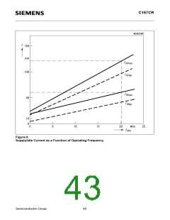
Semiconductor Group
41

 INFINEON [ Infineon ]