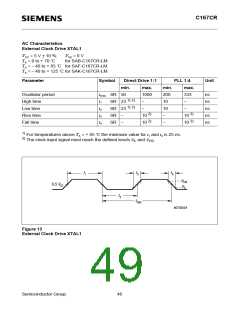
C167CR
Notes
1)
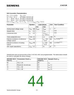
VAIN may exceed VAGND or VAREF up to the absolute maximum ratings. However, the conversion result in these
cases will be X000H or X3FFH, respectively.
2)
3)
During the sample time the input capacitance CI can be charged/discharged by the external source. The
internal resistance of the analog source must allow the capacitance to reach its final voltage level within tS.
After the end of the sample time tS, changes of the analog input voltage have no effect on the conversion result.
Values for the sample clock tSC depend on programming and can be taken from the table above.
This parameter includes the sample time tS, the time for determining the digital result and the time to load the
result register with the conversion result.
Values for the conversion clock tCC depend on programming and can be taken from the table above.
4)
5)
This parameter depends on the ADC control logic. It is not a real maximum value, but rather a fixum.
TUE is tested at VAREF = 5.0 V, VAGND = 0 V, VCC = 4.9 V. It is guaranteed by design characterization for all other
voltages within the defined voltage range.
The specified TUE is guaranteed only if an overload condition (see IOV specification) occurs on maximum 2 not
selected analog input pins and the absolute sum of input overload currents on all analog input pins does not
exceed 10 mA.
During the reset calibration sequence the maximum TUE may be ± 4 LSB.
6)
7)
During the conversion the ADC’s capacitance must be repeatedly charged or discharged. The internal
resistance of the reference voltage source must allow the capacitance to reach its respective voltage level
within tCC. The maximum internal resistance results from the programmed conversion timing.
Not 100 % tested, guaranteed by design characterization.
Semiconductor Group
42

 INFINEON [ Infineon ]