SAE 81C90/91
07Feb95@09:05h Intermediate Version
Bit-Length Registers
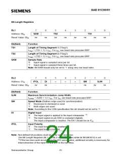
BL1
7
6
5
4
3
2
1
0
Address: 00
SAM
TS2
rw
TS1
H
Reset Value: 00
rw
rw
rw
rw
rw
rw
rw
H
Bit(field)
TS1
Function
Length of Timing Segment 1 (TSeg1).
TSeg1 = (TS1 + 1) × tSCL. For tSCL see baud-rate prescaler BRP.
Length of Timing Segment 2 (TSeg2).
TSeg2 = (TS2 + 1) × tSCL. For tSCL see baud-rate prescaler BRP.
t
TS2
t
SAM
Sample Rate
’0’: Input signal is sampled once per bit.
’1’: Input signal is sampled three times per bit.
Note: Bit SAM should only be set to ’1’ using very low baud rates.
BL2
7
6
5
–
-
4
–
-
3
–
-
2
1
0
Address: 01
IPOL
rw
DI
rw
SM
rw
SJW
H
Reset Value: 00
rw
rw
H
Bit(field)
SJW
Function
Maximum Synchronization Jump Width.
SJWidth = (SJW + 1) × tSCL. For tSCL see baud-rate prescaler BRP.
t
SM
Speed Mode (Defines edge used for synchronization)
’0’: Recessive to dominant is used.
’1’: Both edges are used.
Note: According to the CAN specification this bit should not be set to ’1’.
DI
Digital Input
’0’: The input signal is applied to the input comparator. 1)
’1’: The input signal on pin RX0 is evaluated digitally.
The input comparator is inactive. Pin RX1 should be on VSS
.
IPOL
Input Polarity
’0’: The input level remains unaltered.
’1’: The input level is inverted.
Note: Not defined bit positions must be ’0’ for write accesses.
The Bit Length Registers BL1 and BL2 can only written while bit IM (MOD.0) is set.
1) If the bus lines work according to the ISO specification, additional circuitry is necessary for
interconnection of the input comparator to the bus lines.
Semiconductor Group
23

 INFINEON [ Infineon ]