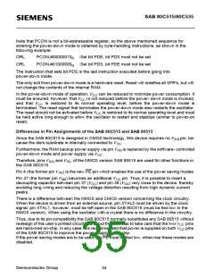
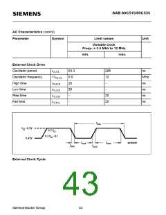
SAB 80C515/80C535
Notes for page 36 and 37:
1) Capacitive loading on ports 0 and 2 may cause spurious noise pulses to be
superimposed on the V of ALE and ports 1, 3, 4 and 5. The noise is due to external bus
OL
capacitance discharging into the port 0 and port 2 pins when these pins make 1-to-0
transitions during bus operation.
In the worst case (capacitive loading > 100 pF), the noise pulse on ALE line may
exceed 0.8 V.
Then, it may be desirable to qualify ALE with a Schmitttrigger, or use an address latch
with a Schmitttrigger strobe input.
2) Capacitive loading on ports 0 and 2 may cause the VOH on ALE and PSEN to
momentarily fall below the 0.9 V specification when the address bits are stabilizing.
CC
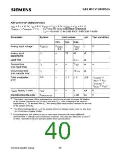
3) Power-down I is measured with: EA = Port 0 = Port 6 = V ;
CC
CC
XTAL1 = N.C.; XTAL2 = V ; RESET = V ; V
= V ; all other pins are disconnected.
SS
SS
CC AGND
4) I (active mode) is measured with: XTAL2 driven with the clock signal according
CC
to the figure below; XTAL1 = N.C.; EA = Port 0 = Port 6 = V ; RESET = V ; all other
CC
SS
pins are disconnected. I might be slightly higher if a crystal oscillator is used.
CC
5) I (idle mode) is measured with: XTAL2 driven with the clock signal according to the
CC
figure below; XTAL1 = N.C.; EA = V ; Port 0 = Port 6 V ; RESET = V ; all other pins are
SS
CC
CC
disconnected; all on-chip peripherals are disabled.
6) I at other frequencies is given by:
CC
Active mode: I
(mA) = 2.67 × f
(MHz) + 3.00
OSC
CC max
Idle mode: I
(mA) = 0.88 × f
(MHz) + 2.50
OSC
CC max
where f
is the oscillator frequency in MHz.
OSC
I
is given in mA and measured at V = 5 V (see also notes 4 and 5)
CC
CC max
Semiconductor Group
38

 INFINEON [ Infineon ]