SAB 80C515/80C535
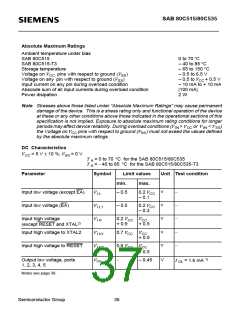
Absolute Maximum Ratings
Ambient temperature under bias
SAB 80C515
0 to 70 °C
SAB 80C515-T3
Storage temperature
– 40 to 85 °C
– 65 to 150 °C
– 0.5 to 6.5 V
Voltage on V
pins with respect to ground (V )
CC
SS
Voltage on any pin with respect to ground (V )
– 0.5 to V + 0.5 V
SS
CC
Input current on any pin during overload condition
Absolute sum of all input currents during overload condition
Power disipation
– 10 mA to + 10 mA
|100 mA|
2 W
Note Stresses above those listed under "Absolute Maximum Ratings" may cause permanent
damage of the device. This is a stress rating only and functional operation of the device
at these or any other conditions above those indicated in the operational sections of this
specification is not implied. Exposure to absolute maximum rating conditions for longer
periods may affect device reliability. During overload conditions (V > V or V < V )
I N
CC
I N
SS
the Voltage on V pins with respect to ground (V ) must not exeed the values defined
CC
SS
by the absolute maximum ratings.
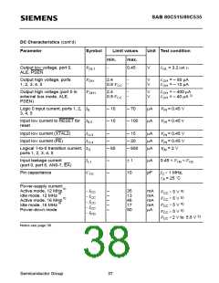
DC Characteristics
= 5 V ± 10 %; V = 0 V
V
CC
SS
T = 0 to 70 °C for the SAB 80C515/80C535
A
T = – 40 to 85 °C for the SAB 80C515/80C535-T3
A
Parameter
Symbol
Limit values
Unit Test condition
min.
max.
V
V
V
V
V
–
–
–
–
–
Input low voltage (except EA)
Input low voltage (EA)
V
V
V
V
V
– 0.5
0.2 V
– 0.1
I L
CC
– 0.5
0.2 V
I L1
I H
CC
– 0.3
Input high voltage
(except RESET and XTAL2)
0.2 V
+ 0.9
V
CC
+ 0.5
CC
CC
CC
Input high voltage to XTAL2
0.7 V
0.6 V
–
V
CC
+ 0.5
I H1
I H2
Input high voltage to RESET
V
CC
+ 0.5
I
= 1.6 mA 1)
Output low voltage, ports
1, 2, 3, 4, 5
V
– 0.45
V
OL
OL
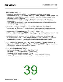
Notes see page 38.
Semiconductor Group
36

 INFINEON [ Infineon ]