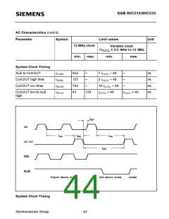
SAB 80C515/80C535
A/D Converter Characteristics
V
V
= 5 V ± 10 %; V = 0 V; V
= V ± 5 %; V
= V ± 0.2 V;
AGND SS
CC
SS
AREF
CC
–V
≥ 1 V;
T = 0 to 70 ˚C for SAB 80C515/80C535
I ntAREF
IntAGND
A
T = – 40 to 85 ˚C for SAB 80C515/80C535-T40/85
A
Parameter
Symbol
Limit values
Unit
Test condition
min.
typ.
max.
–
9)
7)
Analog input voltage
V
C
V
– 0.2
V
AREF
+ 0.2
V
AINPUT
I
AGND
Analog input
capacitance
–
25
45
pF
Load time
t
t
–
–
–
–
2 t
7 t
µs
µs
–
–
L
CY
CY
Sample time
(incl. load time)
S
C
Conversion time
(incl. sample time)
t
–
–
–
13 t
µs
–
CY
TUE
Total unadjusted
error
± 1
± 2
LSB
V
V
V
V
=
I ntAREF
= V
AREF
CC
=
I ntAGND
= V 7)
AGND
SS
8)
8)
V
supply current
I
–
–
–
5
mA
mV
AREF
REF
Internal reference error
V
± 30
I nt REFERR
7)
The output impedance of the analog source must be low enough to assure full loading
of the sample capacitance (C ) during load time (tL ) . After charging of the internal
I
capacitance (CI ) in the load time (tL) the analog input must be held constant for the rest
of the sample time (t )
S
8)
9)
The differential impedance r of the analog reference voltage source must be less than
D
1 kΩ at reference supply voltage.
Exceeding these limit values at one or more input channels will cause additional
current which is sinked / sourced at these channels. This may also affect the accuracy
of other channels which are operated within these specifications.
Semiconductor Group
39

 INFINEON [ Infineon ]