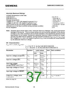
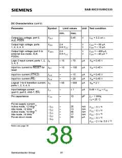
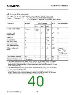
SAB 80C515/80C535
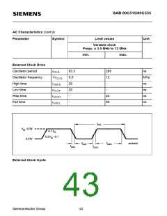
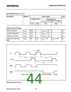
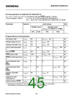
AC Characteristics
= 5 V ± 10%; V = 0 V (CL for Port 0, ALE and PSEN outputs = 100 pF;
V
CC
SS
C for all outputs = 80 pF);
T = 0 to 70 ˚C for SAB 80C515/80C535
L
A
T = – 40 to 85 ˚C for SAB 80C515/80C535-T40/85
A
Parameter
Symbol
Limit values
Unit
12 MHz clock
Variable clock
= 3.5 MHz to 12 MHz
1/t
CLCL
min.
max.
min.
max.
Program Memory Characteristics
ALE pulse width
t
t
t
t
127
–
2 t
– 40
C LCL
–
ns
ns
ns
LHLL
AVLL
LLAX
LLIV
Address setup to ALE
Address hold after ALE
53
48
–
–
t
t
– 30
–
C LCL
C LCL
–
– 35
–
ALE to valid instruction
in
233
–
4 t
– 100 ns
CLCL
C LCL
ALE to PSEN
t
t
58
215
–
–
t
– 25
–
ns
ns
LLPL
PLPH
PLIV
C LCL
PSEN pulse width
3 t
– 35
C LCL
PSEN to valid instruction t
in
150
–
–
3 t
– 100 ns
–
Input instruction hold
after PSEN
t
t
t
0
0
ns
PXIX
1)
–
Input instruction float
after PSEN
–
63
t
– 20
C LCL
ns
ns
PXIZ
)
1
Address valid after
PSEN
75
–
t
– 8
C LCL
PXAV
A VIV
A ZPL
–
Address to valid instruc- t
tion in
302
–
5 t
– 115 ns
ns
C LCL
–
Address float to PSEN
t
0
0
1)
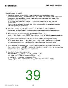
Interfacing the SAB 80C515 to devices with float times up to 75 ns is permissible.
This limited bus contention will not cause any damage to port 0 drivers.
Semiconductor Group
40

 INFINEON [ Infineon ]