S29GL01GP
S29GL512P
S29GL256P
S29GL128P
11.7 AC Characteristics
11.7.1
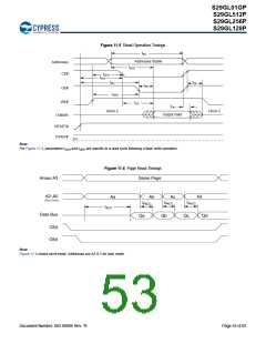
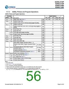
S29GL-P Read Operations
S29GL-P Read Operations
Parameter
Speed Options
90 100 110 120 130 Unit
Description
(Notes)
JEDEC
Std.
Test Setup
VIO = VCC = 2.7 V
–
100 110 120
–
VIO = 1.65 V to VCC
CC = 3 V
,
,
,
tAVAV
tRC Read Cycle Time
Min
Max
Max
–
–
110 120 130 ns
V
VIO = VCC = 3.0 V
VIO = VCC = 2.7 V
VIO = 1.65 V to VCC
90 100 110
–
–
–
–
100 110 120
tAVQV
tACC Address to Output Delay (1)
tCE Chip Enable to Output Delay (2)
–
–
110 120 130 ns
V
CC = 3 V
VIO = VCC = 3.0 V
IO = VCC = 2.7 V
90 100 110
–
–
–
V
–
100 110 120
VIO = 1.65 V to VCC
VCC = 3 V
tELQV
–
–
110 120 130 ns
VIO = VCC = 3.0 V
90 100 110
–
–
tPACC Page Access Time
Max
Max
Max
Max
25
25
20
20
ns
ns
ns
ns
tGLQV
tEHQZ
tGHQZ
tOE Output Enable to Output Delay
tDF Chip Enable to Output High Z (3)
tDF Output Enable to Output High Z (3)
Output Hold Time From Addresses, CE#
or OE#, Whichever Occurs First
tAXQX
tOH
Min
Min
Min
Min
0
0
ns
ns
ns
ns
Read
Output Enable Hold Time
(3)
tOEH
Toggle and
Data# Polling
10
35
tCEH Chip Enable Hold Time
Read
Notes
1. CE#, OE# = VIL
2. OE# = VIL
3. Not 100% tested.
4. See Figure 11.3 and Table for test specifications.
5. Unless otherwise indicated, AC specifications for 110 ns speed options are tested with VIO = VCC = 2.7 V. AC specifications for 110 ns speed
options are tested with VIO = 1.8 V and VCC = 3.0 V.
Document Number: 002-00886 Rev. *B
Page 52 of 83

 INFINEON [ Infineon ]