S29GL01GP
S29GL512P
S29GL256P
S29GL128P
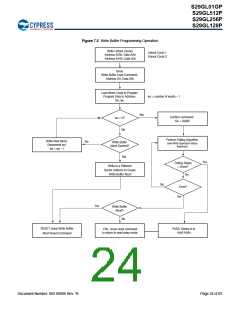
Write buffer programming is allowed in any sequence of memory (or address) locations. These flash devices are capable of handling
multiple write buffer programming operations on the same write buffer address range without intervening erases.
Use of the write buffer is strongly recommended for programming when multiple words are to be programmed.
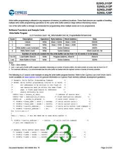
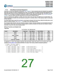
Software Functions and Sample Code
Write Buffer Program
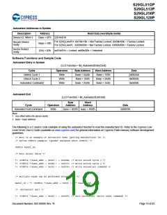
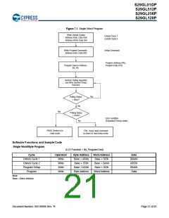
(LLD Functions Used = lld_WriteToBufferCmd, lld_ProgramBufferToFlashCmd)
Cycle
Description
Unlock
Operation Byte Address Word Address
Data
00AAh
1
2
3
4
Write
Write
Write
Write
Base + AAAh
Base + 555h
Base + 555h
Base + 2AAh
Unlock
0055h
Write Buffer Load Command
Write Word Count
Sector Address
Sector Address
0025h
Word Count (N–1)h
Number of words (N) loaded into the write buffer can be from 1 to 32 words (1 to 64 bytes).
5 to 36
Last
Load Buffer Word N
Write Buffer to Flash
Write
Write
Program Address, Word N
Sector Address
Word N
0029h
Notes
1. Base = Base Address.
2. Last = Last cycle of write buffer program operation; depending on number of words written, the total number of cycles may be from 6 to 37.
3. For maximum efficiency, it is recommended that the write buffer be loaded with the highest number of words (N words) possible.
The following is a C source code example of using the write buffer program function. Refer to the Cypress Low Level Driver User’s
Guide (available on www.cypress.com) for general information on Cypress Flash memory software development guidelines.
/* Example: Write Buffer Programming Command
*/
/* NOTES: Write buffer programming limited to 16 words. */
/*
/*
/*
/*
All addresses to be written to the flash in
one operation must be within the same flash
page. A flash page begins at addresses
evenly divisible by 0x20.
*/
*/
*/
*/
UINT16 *src = source_of_data;
/* address of source data
/* flash destination address
/* word count (minus 1)
/* write unlock cycle 1
/* write unlock cycle 2
*/
*/
UINT16 *dst = destination_of_data;
UINT16 wc
= words_to_program -1;
*/
*/
*/
*( (UINT16 *)base_addr + 0x555 ) = 0x00AA;
*( (UINT16 *)base_addr + 0x2AA ) = 0x0055;
*( (UINT16 *)sector_address )
*( (UINT16 *)sector_address )
= 0x0025;
= wc;
/* write write buffer load command */
/* write word count (minus 1) */
for (i=0;i<=wc;i++)
{
*dst++ = *src++; /* ALL dst MUST BE in same Write Buffer */
}
*( (UINT16 *)sector_address )
/* poll for completion */
= 0x0029;
/* write confirm command
*/
/* Example: Write Buffer Abort Reset */
*( (UINT16 *)addr + 0x555 ) = 0x00AA;
*( (UINT16 *)addr + 0x2AA ) = 0x0055;
*( (UINT16 *)addr + 0x555 ) = 0x00F0;
/* write unlock cycle 1
/* write unlock cycle 2
/* write buffer abort reset
*/
*/
*/
Document Number: 002-00886 Rev. *B
Page 23 of 83

 INFINEON [ Infineon ]