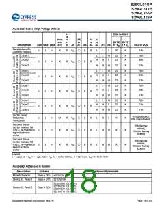
S29GL01GP
S29GL512P
S29GL256P
S29GL128P
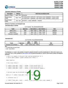
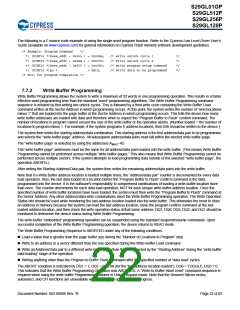
The following is a C source code example of using the single word program function. Refer to the Cypress Low Level Driver User’s
Guide (available on www.cypress.com) for general information on Cypress Flash memory software development guidelines.
/* Example: Program Command
*/
*( (UINT16 *)base_addr + 0x555 ) = 0x00AA;
*( (UINT16 *)base_addr + 0x2AA ) = 0x0055;
*( (UINT16 *)base_addr + 0x555 ) = 0x00A0;
/* write unlock cycle 1
*/
*/
*/
*/
/* write unlock cycle 2
/* write program setup command
/* write data to be programmed
*( (UINT16 *)pa )
= data;
/* Poll for program completion */
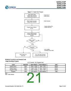
7.7.2
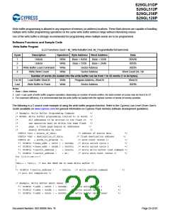
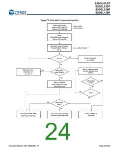
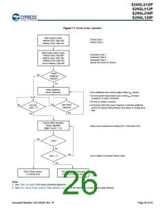
Write Buffer Programming
Write Buffer Programming allows the system to write a maximum of 32 words in one programming operation. This results in a faster
effective word programming time than the standard “word” programming algorithms. The Write Buffer Programming command
sequence is initiated by first writing two unlock cycles. This is followed by a third write cycle containing the Write Buffer Load
command written at the Sector Address in which programming occurs. At this point, the system writes the number of “word locations
minus 1” that are loaded into the page buffer at the Sector Address in which programming occurs. This tells the device how many
write buffer addresses are loaded with data and therefore when to expect the “Program Buffer to Flash” confirm command. The
number of locations to program cannot exceed the size of the write buffer or the operation aborts. (Number loaded = the number of
locations to program minus 1. For example, if the system programs 6 address locations, then 05h should be written to the device.)
The system then writes the starting address/data combination. This starting address is the first address/data pair to be programmed,
and selects the “write-buffer-page” address. All subsequent address/data pairs must fall within the elected write-buffer-page.
The “write-buffer-page” is selected by using the addresses AMAX–A5.
The “write-buffer-page” addresses must be the same for all address/data pairs loaded into the write buffer. (This means Write Buffer
Programming cannot be performed across multiple “write-buffer-pages.” This also means that Write Buffer Programming cannot be
performed across multiple sectors. If the system attempts to load programming data outside of the selected “write-buffer-page”, the
operation ABORTs.)
After writing the Starting Address/Data pair, the system then writes the remaining address/data pairs into the write buffer.
Note that if a Write Buffer address location is loaded multiple times, the “address/data pair” counter is decremented for every data
load operation. Also, the last data loaded at a location before the “Program Buffer to Flash” confirm command is the data
programmed into the device. It is the software's responsibility to comprehend ramifications of loading a write-buffer location more
than once. The counter decrements for each data load operation, NOT for each unique write-buffer-address location. Once the
specified number of write buffer locations have been loaded, the system must then write the “Program Buffer to Flash” command at
the Sector Address. Any other address/data write combinations abort the Write Buffer Programming operation. The Write Operation
Status bits should be used while monitoring the last address location loaded into the write buffer. This eliminates the need to store
an address in memory because the system can load the last address location, issue the program confirm command at the last
loaded address location, and then check the write operation status at that same address. DQ7, DQ6, DQ5, DQ2, and DQ1 should be
monitored to determine the device status during Write Buffer Programming.
The write-buffer “embedded” programming operation can be suspended using the standard suspend/resume commands. Upon
successful completion of the Write Buffer Programming operation, the device returns to READ mode.
The Write Buffer Programming Sequence is ABORTED under any of the following conditions:
Load a value that is greater than the page buffer size during the “Number of Locations to Program” step.
Write to an address in a sector different than the one specified during the Write-Buffer-Load command.
Write an Address/Data pair to a different write-buffer-page than the one selected by the “Starting Address” during the “write buffer
data loading” stage of the operation.
Writing anything other than the Program to Buffer Flash Command after the specified number of “data load” cycles.
The ABORT condition is indicated by DQ1 = 1, DQ7 = DATA# (for the “last address location loaded”), DQ6 = TOGGLE, DQ5 = 0.
This indicates that the Write Buffer Programming Operation was ABORTED. A “Write-to-Buffer-Abort reset” command sequence is
required when using the write buffer Programming features in Unlock Bypass mode. Note that the Secured Silicon sector,
autoselect, and CFI functions are unavailable when a program operation is in progress.
Document Number: 002-00886 Rev. *B
Page 22 of 83

 INFINEON [ Infineon ]