S29GL01GP
S29GL512P
S29GL256P
S29GL128P
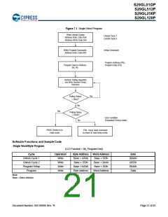
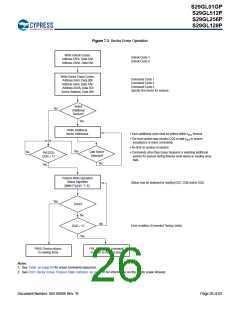
7.7.3
Sector Erase
The sector erase function erases one or more sectors in the memory array. (See Table on page 65 and Figure 7.3.) The device
does not require the system to preprogram a sector prior to erase. The Embedded Erase algorithm automatically programs and
verifies the entire memory to an all zero data pattern prior to electrical erase. After a successful sector erase, all locations within the
erased sector contain FFFFh. The system is not required to provide any controls or timings during these operations.
After the command sequence is written, the sector erase time-out tSEA (50 µs) occurs. During the time-out period, additional sector
addresses may be written. Loading the sector erase buffer may be done in any sequence, and the number of sectors may be from
one sector to all sectors. The time between these additional cycles must be less than 50 µs. Any sector erase address and
command following the exceeded time-out (50 µs) may or may not be accepted. Any command other than Sector Erase or Erase
Suspend during the time-out period resets that sector to the read mode. The system can monitor DQ3 to determine if the sector
erase timer has timed out (See Section 7.8.6.) The time-out begins from the rising edge of the final WE# pulse in the command
sequence.
When the Embedded Erase algorithm is complete, the sector returns to reading array data and addresses are no longer latched.
The system can determine the status of the erase operation by reading DQ7 or DQ6/DQ2 in the erasing sector. Refer to Section 7.8
for information on these status bits.
Once the sector erase operation has begun, only the Erase Suspend command is valid. All other commands are ignored. However,
note that a hardware reset immediately terminates the erase operation. If that occurs, the sector erase command sequence should
be reinitiated once that sector has returned to reading array data, to ensure the sector is properly erased.
The Unlock Bypass feature allows the host system to send program commands to the Flash device without first writing unlock cycles
within the command sequence. See Section 7.7.8 for details on the Unlock Bypass function.
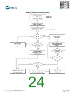
Figure 7.3 illustrates the algorithm for the erase operation. Refer to Section 11.7.5 for parameters and timing diagrams.
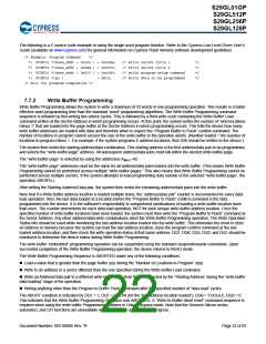
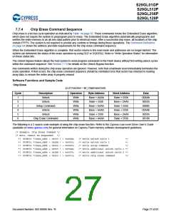
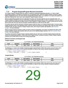
Software Functions and Sample Code
Sector Erase
(LLD Function = lld_SectorEraseCmd)
Operatio
Cycle
Description
Unlock
n
Byte Address
Base + AAAh
Base + 555h
Base + AAAh
Base + AAAh
Base + 555h
Word Address
Base + 555h
Base + 2AAh
Base + 555h
Base + 555h
Base + 2AAh
Data
00AAh
0055h
0080h
00AAh
0055h
0030h
1
2
3
4
5
6
Write
Write
Write
Write
Write
Write
Unlock
Setup Command
Unlock
Unlock
Sector Erase Command
Sector Address Sector Address
Unlimited additional sectors may be selected for erase; command(s) must be written within 50 µs.
The following is a C source code example of using the sector erase function. Refer to the Cypress Low Level Driver User’s Guide
(available on www.cypress.com) for general information on Cypress Flash memory software development guidelines.
/* Example: Sector Erase Command */
*( (UINT16 *)base_addr + 0x555 ) = 0x00AA;
*( (UINT16 *)base_addr + 0x2AA ) = 0x0055;
*( (UINT16 *)base_addr + 0x555 ) = 0x0080;
*( (UINT16 *)base_addr + 0x555 ) = 0x00AA;
*( (UINT16 *)base_addr + 0x2AA ) = 0x0055;
/* write unlock cycle 1
/* write unlock cycle 2
/* write setup command
*/
*/
*/
/* write additional unlock cycle 1 */
/* write additional unlock cycle 2 */
*( (UINT16 *)sector_address )
= 0x0030;
/* write sector erase command
*/
Document Number: 002-00886 Rev. *B
Page 25 of 83

 INFINEON [ Infineon ]