S29GL01GP
S29GL512P
S29GL256P
S29GL128P
7.7.4
Chip Erase Command Sequence
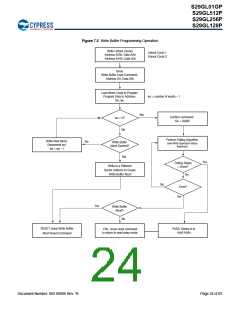
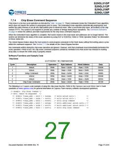
Chip erase is a six-bus cycle operation as indicated by Table on page 65. These commands invoke the Embedded Erase algorithm,
which does not require the system to preprogram prior to erase. The Embedded Erase algorithm automatically preprograms and
verifies the entire memory to an all zero data pattern prior to electrical erase. After a successful chip erase, all locations of the chip
contain FFFFh. The system is not required to provide any controls or timings during these operations. The Command Definitions
on page 64 shows the address and data requirements for the chip erase command sequence.
When the Embedded Erase algorithm is complete, that sector returns to the read mode and addresses are no longer latched. The
system can determine the status of the erase operation by using DQ7 or DQ6/DQ2. Refer to “Write Operation Status” for information
on these status bits.
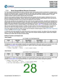
The Unlock Bypass feature allows the host system to send program commands to the Flash device without first writing unlock cycles
within the command sequence. See Section 7.7.8 for details on the Unlock Bypass function.
Any commands written during the chip erase operation are ignored. However, note that a hardware reset immediately terminates the
erase operation. If that occurs, the chip erase command sequence should be reinitiated once that sector has returned to reading
array data, to ensure the entire array is properly erased.
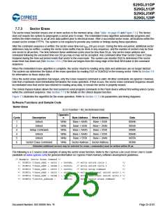
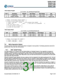
Software Functions and Sample Code
Chip Erase
(LLD Function = lld_ChipEraseCmd)
Cycle
Description
Unlock
Operation
Write
Byte Address
Base + AAAh
Base + 555h
Base + AAAh
Base + AAAh
Base + 555h
Base + AAAh
Word Address
Base + 555h
Base + 2AAh
Base + 555h
Base + 555h
Base + 2AAh
Base + 555h
Data
00AAh
0055h
0080h
00AAh
0055h
0010h
1
2
3
4
5
6
Unlock
Write
Setup Command
Unlock
Write
Write
Unlock
Write
Chip Erase Command
Write
The following is a C source code example of using the chip erase function. Refer to the Cypress Low Level Driver User’s Guide
(available on www.cypress.com) for general information on Cypress Flash memory software development guidelines.
/* Example: Chip Erase Command */
/* Note: Cannot be suspended
*/
*( (UINT16 *)base_addr + 0x555 ) = 0x00AA;
*( (UINT16 *)base_addr + 0x2AA ) = 0x0055;
*( (UINT16 *)base_addr + 0x555 ) = 0x0080;
*( (UINT16 *)base_addr + 0x555 ) = 0x00AA;
*( (UINT16 *)base_addr + 0x2AA ) = 0x0055;
*( (UINT16 *)base_addr + 0x555 ) = 0x0010;
/* write unlock cycle 1
/* write unlock cycle 2
/* write setup command
*/
*/
*/
/* write additional unlock cycle 1 */
/* write additional unlock cycle 2 */
/* write chip erase command
*/
Document Number: 002-00886 Rev. *B
Page 27 of 83

 INFINEON [ Infineon ]