S29GL01GP
S29GL512P
S29GL256P
S29GL128P
7.7
Program/Erase Operations
These devices are capable of several modes of programming and or erase operations which are described in detail in the following
sections.
During a write operation, the system must drive CE# and WE# to VIL and OE# to VIH when providing address, command, and data.
Addresses are latched on the last falling edge of WE# or CE#, while data is latched on the 1st rising edge of WE# or CE#.
The Unlock Bypass feature allows the host system to send program commands to the Flash device without first writing unlock cycles
within the command sequence. See Section 7.7.8 for details on the Unlock Bypass function.
Note the following:
When the Embedded Program algorithm is complete, the device returns to the read mode.
The system can determine the status of the program operation by reading the DQ status bits. Refer to the Write Operation Status
on page 32 for information on these status bits.
An “0” cannot be programmed back to a “1.” A succeeding read shows that the data is still “0.”
Only erase operations can convert a “0” to a “1.”
Any commands written to the device during the Embedded Program/Erase are ignored except the Suspend commands.
Secured Silicon Sector, Autoselect, and CFI functions are unavailable when a program operation is in progress.
A hardware reset and/or power removal immediately terminates the Program/Erase operation and the Program/Erase command
sequence should be reinitiated once the device has returned to the read mode to ensure data integrity.
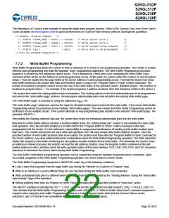
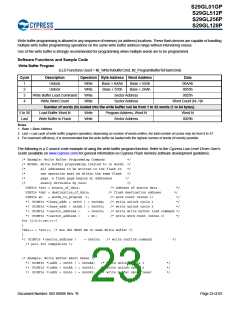
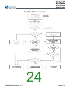
Programming is allowed in any sequence and across sector boundaries for single word programming operation. See Write Buffer
Programming on page 23 when using the write buffer.
Programming to the same word address multiple times without intervening erases is permitted.
7.7.1
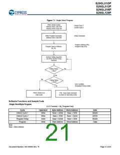
Single Word Programming
Single word programming mode is one method of programming the Flash. In this mode, four Flash command write cycles are used
to program an individual Flash address. The data for this programming operation could be 8 or 16-bits wide.
While the single word programming method is supported by most Cypress devices, in general Single Word Programming is not
recommended for devices that support Write Buffer Programming. See Table on page 65 for the required bus cycles and Figure 7.1
for the flowchart.
When the Embedded Program algorithm is complete, the device then returns to the read mode and addresses are no longer latched.
The system can determine the status of the program operation by reading the DQ status bits. Refer to Write Operation Status
on page 32 for information on these status bits.
During programming, any command (except the Suspend Program command) is ignored.
The Secured Silicon Sector, Autoselect, and CFI functions are unavailable when a program operation is in progress.
A hardware reset immediately terminates the program operation. The program command sequence should be reinitiated once the
device has returned to the read mode, to ensure data integrity.
Programming to the same address multiple times continuously (for example, “walking” a bit within a word) is permitted.
Document Number: 002-00886 Rev. *B
Page 20 of 83

 INFINEON [ Infineon ]