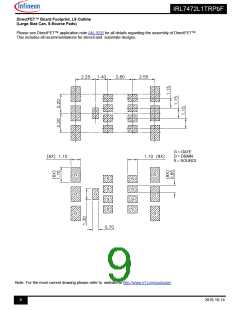
IRL7472L1TRPbF
Dynamic @ TJ = 25°C (unless otherwise specified)
Symbol
Parameter
Forward Transconductance
Total Gate Charge
Min. Typ. Max. Units
Conditions
DS = 10V, ID = 195A
gfs
Qg
232 ––– –––
––– 220 330
S
V
ID = 195A
Qgs
Qgd
Qsync
td(on)
tr
td(off)
tf
Ciss
Coss
Crss
Gate-to-Source Charge
Gate-to-Drain ("Miller") Charge
Total Gate Charge Sync. (Qg - Qgd)
Turn-On Delay Time
Rise Time
Turn-Off Delay Time
Fall Time
Input Capacitance
Output Capacitance
Reverse Transfer Capacitance
–––
–––
95
87
–––
–––
VDS = 20V
nC
VGS = 4.5V
ID = 195A, VDS =0V, VGS = 4.5V
VDD = 20V
ID = 30A
RG = 2.7
––– 133 –––
––– 68 –––
––– 176 –––
––– 174 –––
––– 137 –––
––– 20082 –––
––– 2436 –––
––– 1594 –––
ns
VGS = 4.5V
VGS = 0V
VDS = 25V
ƒ = 10kHz
pF
C
C
oss eff. (ER) Effective Output Capacitance (Energy Related) ––– 2855 –––
oss eff. (TR) Effective Output Capacitance (Time Related) ––– 3544 –––
VGS = 0V, VDS = 0V to 32V
VGS = 0V, VDS = 0V to 32V
Diode Characteristics
Symbol Parameter
Min. Typ. Max. Units
Conditions
IS
Continuous Source Current
(Body Diode)
Pulsed Source Current
(Body Diode)
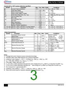
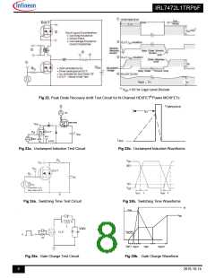
MOSFET symbol
showing the
integral reverse
p-n junction diode.
D
––– –––
341
A
G
ISM
––– –––
––– –––
1500
1.2
S
VSD
Diode Forward Voltage
V
TJ= 25°C, IS =195A, VGS = 0V
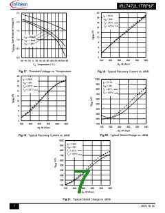
dv/dt
Peak Diode Recovery
TJ =175°C, IS =195A,
VDS = 40V
––– 1.3
–––
V/ns
trr
Reverse Recovery Time
–––
–––
––– 103
––– 114
––– 3.1
57
58
–––
–––
–––
–––
–––
TJ = 25° C VR = 34V,
ns
IF = 195A
TJ = 125°C
TJ = 25°C
TJ = 125°C
TJ = 25°C
di/dt = 100A/µs
Qrr
IRRM
Reverse Recovery Charge
Reverse Recovery Current
nC
A
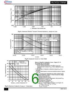
Notes:
Package limit current based on source connection technology
Repetitive rating; pulse width limited by max. junction temperature.
Limited by TJmax, starting TJ = 25°C, L = 0.016mH, RG = 50, IAS = 195A, VGS =10V.
ISD ≤ 195A, di/dt ≤ 984A/µs, VDD ≤ V(BR)DSS, TJ ≤ 175°C.
Pulse width ≤ 400µs; duty cycle ≤ 2%.
Coss eff. (TR) is a fixed capacitance that gives the same charging time as Coss while VDS is rising from 0 to 80% VDSS
.
Coss eff. (ER) is a fixed capacitance that gives the
R is measured at TJ approximately 90°C.
same energy as Coss while VDS is rising from 0 to 80% VDSS.
Limited by TJmax, starting TJ = 25°C, L = 1.0mH, RG = 50, IAS = 39A, VGS =10V.
Silicon limit current based on maximum allowable junction temperature TJmax.
3
2016-10-14

 INFINEON [ Infineon ]