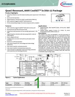
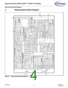
Quasi-Resonant, 800V CoolSET™ in DS0-12 Package
Pin Configuration and Functionality
1
Pin Configuration and Functionality
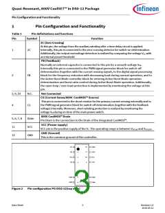
Table 1
Pin
Pin definitations and functions
Symbol
Function
ZC (Zero Crossing)
At this pin, the voltage from the auxiliary winding after a time delay circuit is applied.
Internally, this pin is connected to the zero-crossing detector for switch-on determination.
Additionally, the output overvoltage detection is realized by comparing the voltage VZC with
an internal preset threshold.
1
2
ZC
FB (Feedback)
Normally an external capacitor is connected to this pin for a smooth voltage VFB.
Internally this pin is connected to the PWM signal generator block for switch-off
determination (together with the current sensing signal), to the digital signal processing
block for the frequency reduction with decreasing load during normal operation, and to
the Active Burst Mode controller block for entering Active Burst Mode operation
determination and burst ratio control during Active Burst Mode operation. Additionally,
the open-loop / over-load protection is implemented by monitoring the voltage at this
pin.
FB
3, 9, 10
4
N.C.
CS
Not Connected
CS (Current Sense/800V CoolMOS™ Source)
This pin is connected to the shunt resistor for the primary current sensing externally and to
the PWM signal generator block for switch-off determination (together with the feedback
voltage) internally. Moreover, short-winding protection is realized by monitoring the
voltage VCSduring on-time of the main power switch.
800V CoolMOS™Drain
Pin Drain is the connection to the Drain of the integrated CoolMOS™.
5, 6, 7, 8
11
Drain
VCC
VCC (Power supply)
VCC pin is the positive supply of the IC. The operating range is between VVCCoff and VVCCOVP
.
GND (Ground)
This is the common ground of the controller.
12
GND
1
2
3
12
11
10
ZC
FB
GND
VCC
N.C.
N.C.
N.C.
CS
4
9
5
6
8
7
Drain
Drain
Drain
Drain
Figure 2
Pin configuration PG-DSO-12(top view)
Data Sheet
3
Revision 1.0
2016-05-12

 INFINEON [ Infineon ]