AN985B/BX
Registers and Descriptors Description
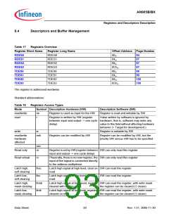
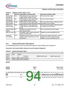
Table 18
Mode
Registers Access Types (cont’d)
Symbol Description Hardware (HW)
Description Software (SW)
Interrupt high,
self clearing
ihsc
Differentiate the input signal (low-
>high) register cleared on read
SW can read the register
Interrupt low,
self clearing
ilsc
Differentiate the input signal (high-
>low) register cleared on read
SW can read the register
Interrupt high,
mask clearing
Interrupt low,
mask clearing
ihmk
ilmk
Differentiate the input signal (high-
SW can read the register, with write mask
>low) register cleared with written mask the register can be cleared
Differentiate the input signal (low-
>high) register cleared with written
mask
SW can read the register, with write mask
the register can be cleared
Interrupt enable ien
register
latch_on_reset lor
Enables the interrupt source for
interrupt generation
rw register, value is latched after first
clock cycle after reset
SW can read and write this register
Register is read and writable by SW
Read/write
self clearing
rwsc
Register is used as input for the hw, the Writing to the register generates a strobe
register will be cleared due to a HW
mechanism.
signal for the HW (1 pdi clock cycle)
Register is read and writable by SW.
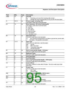
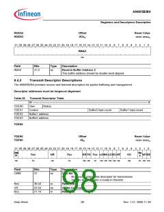
8.4.1
Receive Descriptor Descriptions
The AN985B/BX provides receive and transmit descriptors for packet buffering and management.
Descriptors and receive buffers addresses must be longword alignment
Table 19
Receive Descriptor Table
31 ----------------------------------------------------------------------------------------------------------------------------- 0
RDES0
RDES1
RDES2
RDES3
Own
Status
---
Control
Buffer2 byte-count
Buffer1 byte-count
Buffer1 address (DW boundary)
Buffer2 address (DW boundary)
RDES0
RDES0
RDES0
Offset
00H
Reset Value
xxxx xxxxH
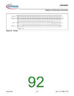
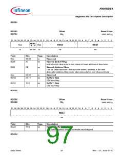
ꢀꢁ ꢀꢂ ꢃꢄ ꢃꢅ ꢃꢆ ꢃꢇ ꢃꢈ ꢃꢉ ꢃꢀ ꢃꢃ ꢃꢁ ꢃꢂ ꢁꢄ ꢁꢅ ꢁꢆ ꢁꢇ ꢁꢈ ꢁꢉ ꢁꢀ ꢁꢃ ꢁꢁ ꢁꢂ ꢄ
ꢅ
ꢆ
ꢇ
ꢈ
ꢉ
ꢀ
ꢃ ꢁ ꢂ
2:
5H
V
)/
(6 '( '7 5) 0) )6 /6 7/ &6 )75:
'%&( 2)
1
UZ
UZ
UZ UZ UZ UZ UZ UZ UZ UZ UZ UZ UZ UR UZ UZ UZ
Data Sheet
94
Rev. 1.51, 2005-11-30

 INFINEON [ Infineon ]