AN985B/BX
Registers and Descriptors Description
8.2.1
PCI/CARDBUS Control/Status Registers Description
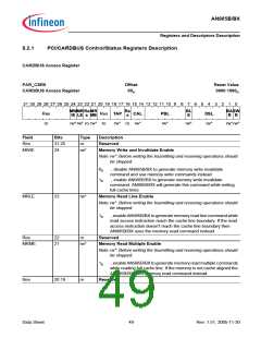
CARDBUS Access Register
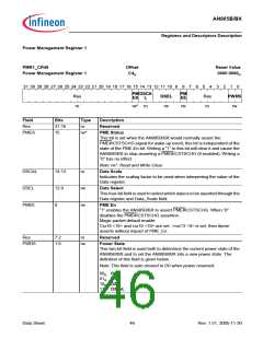
PAR_CSR0
CARDBUS Access Register
Offset
00H
Reset Value
0000 1000H
ꢀꢁ ꢀꢂ ꢃꢄ ꢃꢅ ꢃꢆ ꢃꢇ ꢃꢈ ꢃꢉ ꢃꢀ ꢃꢃ ꢃꢁ ꢃꢂ ꢁꢄ ꢁꢅ ꢁꢆ ꢁꢇ ꢁꢈ ꢁꢉ ꢁꢀ ꢁꢃ ꢁꢁ ꢁꢂ ꢄ
ꢅ
ꢆ
ꢇ
ꢈ
ꢉ
ꢀ ꢃ ꢁ ꢂ
0:055H05
,( /( V 0(
5H
V
%/
(
%$6:
5 5
5HV
UR
5HV 7$3
&$/
3%/
'6/
UZꢊ
UZꢊUZꢊ UR UZꢊ UR
UZꢊ UR UZꢊ
UZꢊ
UZꢊ
UZꢊUZꢊ
Field
Res
MWIE
Bits
31:25
24
Type
ro
rw*
Description
Reserved
Memory Write and Invalidate Enable
Note:rw*: Before writing the trasmitting and receiving operations should
be stopped.
0B
, disable AN985B/BX to generate memory write invalidate
command and use memory write commands instead
, enable AN985B/BX to generate memory write invalidate
command. AN985B/BX will generate this command while writing
full cache lines
1B
MRLE
23
rw*
Memory Read Line Enable
Note:rw*: Before writing the trasmitting and receiving operations should
be stopped.
1B
, enable AN985B/BX to generate memory read line command while
read access instruction reach the cache line boundary. If the read
access instruction doesn’t reach the cache line boundary then
AN985B/BX uses the memory read command instead.
Res
MRME
22
21
ro
rw*
Reserved
Memory Read Multiple Enable
Note:rw*: Before writing the trasmitting and receiving operations should
be stopped.
1B
, enable AN985B/BX to generate memory read multiple commands
while reading full cache line. If the memory is not cache aligned the
AN985B/BX uses memory read command instead.
Res
20:19
ro
Reserved
Data Sheet
49
Rev. 1.51, 2005-11-30

 INFINEON [ Infineon ]